Silicon Photonics and the Future of AI Interconnects
Key Takeaways
The rapid evolution of artificial intelligence models is pushing traditional data center infrastructure to its physical limits, necessitating a transition to optical communication.
- Silicon photonics replaces electron propagation with light, solving the energy and bandwidth bottlenecks inherent in copper wiring.
- Data centers can achieve superior performance by moving optics closer to processing units, effectively eliminating long-distance electrical signal degradation.
- The shift requires standardized manufacturing processes to balance high-volume yield with the precision needed for nanometer-scale photonic integration.
- Optical interconnects enable the massive, rack-scale synchronization necessary for training next-generation large language models efficiently.
- Future infrastructure depends on successfully migrating from legacy electrical networking to cohesive photonic switching and compute engine fabrics.
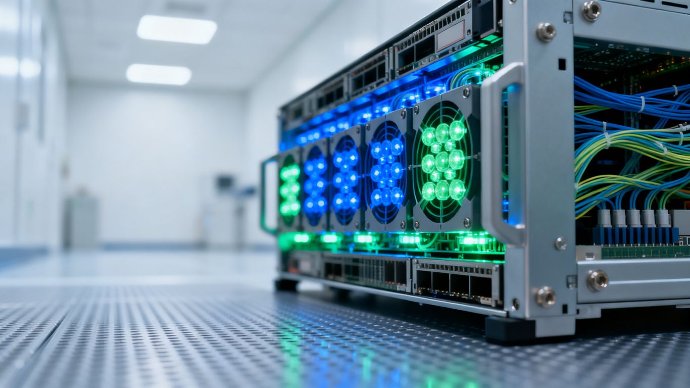
The challenge of AI scalability in data centers
Bottlenecks in traditional electrical interconnects
Modern artificial intelligence demands a level of data throughput that electronic signaling struggles to sustain over distance. As copper wires carry signals, they experience resistive heat loss and electromagnetic interference, forcing engineers to prioritize signal integrity over density. This physical reality creates a bottleneck, as the speed of light in optical mediums remains significantly more efficient than the transmission of electrons through dense metal traces.
Exponential growth of GPU communication requirements
Modern clusters require constant, high-speed information exchange between thousands of processing units to maintain model convergence. Leading solutions like NVIDIA's high-performance networking technology aim to address this volume, as current electrical interconnects introduce systemic lag that prevents full utilization of theoretical compute performance. When communication capacity fails to scale linearly with processing power, the entire cluster faces a proportional drop in efficiency.
Thermal constraints and power consumption limits
Large hyper-scale facilities are approaching power limits that threaten to stall infrastructure expansion. Driving signals electrically across high-speed interfaces generates significant parasitic heat, which necessitates complex, dedicated cooling, accounting for a ballooning share of secondary energy costs.
Latency issues in large-scale AI cluster networking
Network synchronization latency often dictates the runtime for massive AI training jobs. Even nanosecond delays during the weight updates across nodes aggregate into significant operational inefficiencies, which is why silicon photonics ai is being explored as the definitive path to achieving real-time synchronization across sprawling clusters.
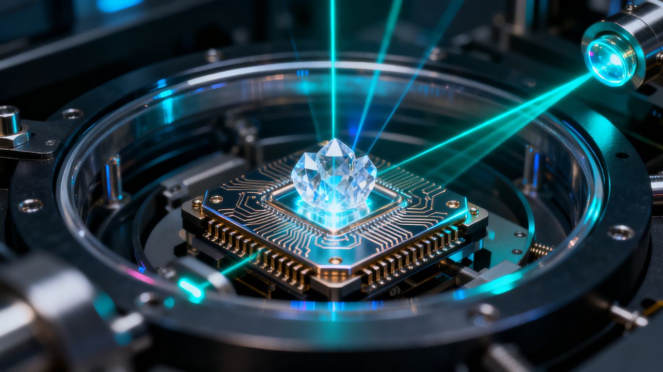
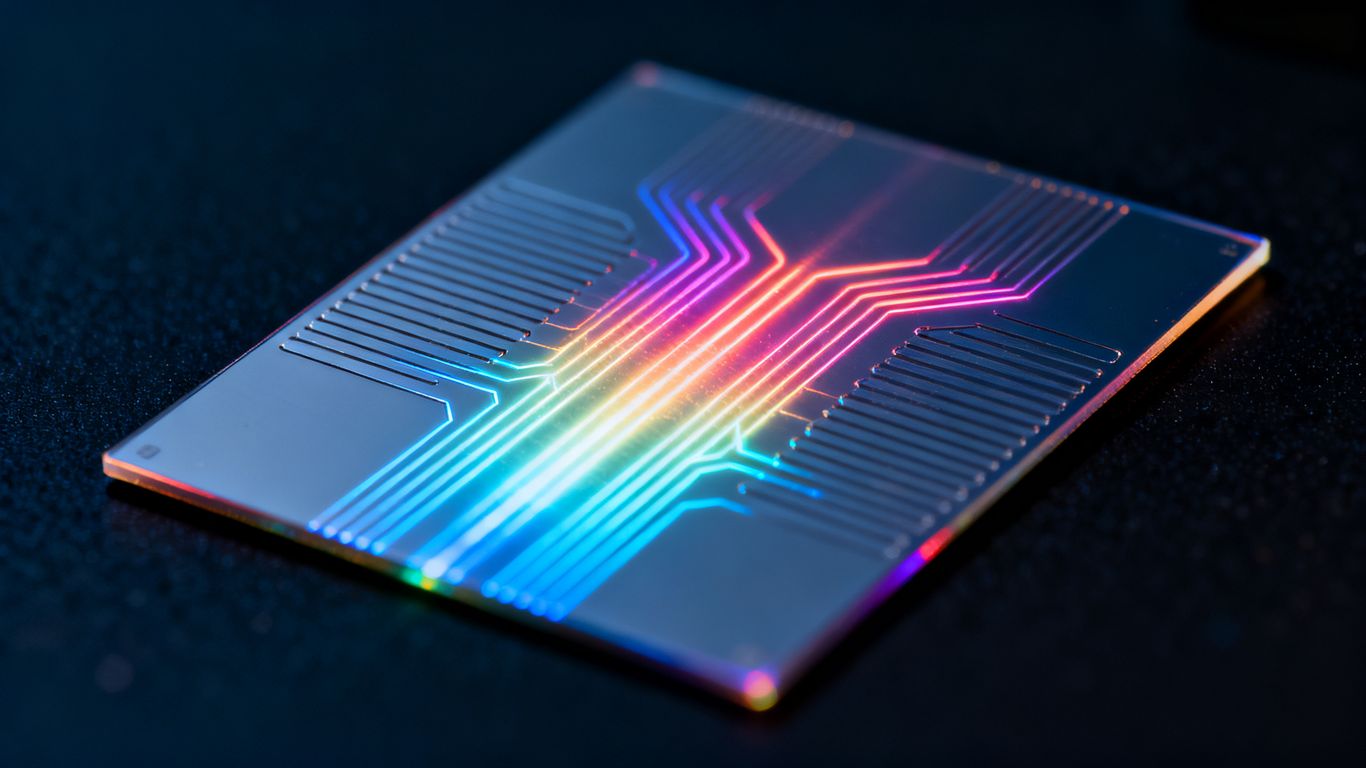
Understanding silicon photonics technology
Core principles of optical data transmission
Optical data transmission relies on generating, modulating, and receiving light signals that carry encoded information through silicon waveguides. Unlike traditional wires, these signals maintain energy efficiency over much greater distances, avoiding the radiative heat generation typical of resistive copper circuitry.
Advantages of using silicon as a photonic platform
Leveraging silicon as a substrate allows for the mass production of photonic components using established semiconductor fabrication nodes. This approach provides a significant cost advantage and allows for the integration of photonic devices with CMOS logic on the same footprint.
Key components: lasers, modulators, and detectors
Integrated photonic circuits require on-chip laser sources, high-bandwidth modulators, and sensitive photodetectors to convert light back into electrical information. These elements must be tightly coupled to minimize coupling losses and footprint, requiring advanced packaging techniques.
CMOS compatibility and manufacturing scalability
By utilizing existing foundry infrastructure, developers can achieve the economy of scale necessary to deploy photonic transceivers globally. As seen in modern photonic progress, this strategy allows industry designers to fold optical capabilities directly into the standard hardware lifecycle without forcing disparate manufacturing paths.
Performance advantages for AI workloads
Achieving superior bandwidth density
Optical interconnects offer an order of magnitude increase in bandwidth per square millimeter compared to traditional electrical pins. This density enables designers to consolidate more data paths into tighter spatial constraints, providing the necessary throughput for high-memory-bandwidth AI chips.
Reducing energy consumption per bit
Transmission of data as light photons requires significantly less energy per distance compared to pushing electrons down conductive metal channels. This fundamental efficiency improvement is a critical factor for sustainable scaling in data center environments where power budget acts as the primary governor of rack density.
Enhancing data reach for distributed compute nodes
Distributing data across high-performance compute nodes usually introduces signficant signal degradation at standard electrical speeds. Optical reach allows for vastly larger cluster topologies, effectively decoupling physical distance from signal timing constraints.
Enabling low-latency synchronization across GPU clusters
Low-latency synchronization is essential for keeping high-performance processors in lockstep during intensive model training tasks.
| Attribute | Electrical Interconnect | Optical Interconnect |
|---|---|---|
| Energy Efficiency | High Loss | Very Low Loss |
| Bandwidth Capacity | Limited | Extremely High |
| Signal Reach | Short Range | Long Range |
| Heat Generation | Significant | Negligible |
This table illustrates the fundamental shift occurring in cluster design. Engineers who prioritize scaling rely on these distinct performance profiles to manage the massive payloads required for agentic AI workloads.
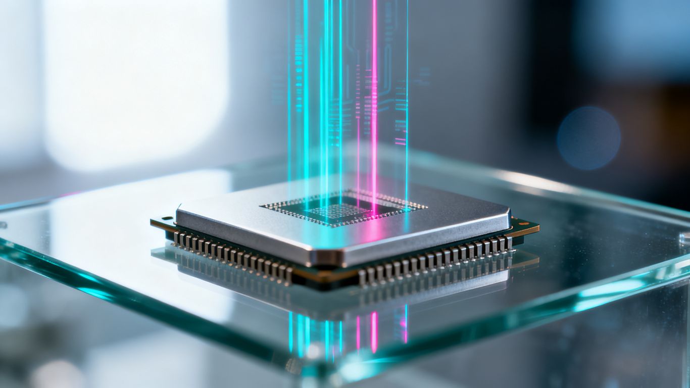
Architectural integration of silicon photonics in AI
Chip-to-chip optical communication
Directly integrating light-based interfaces into the processor package reduces the distance data must travel before hitting an optical link. Technologies like the Cerebras Wafer-Scale Engine have pioneered unique approaches to internal fabric efficiency, and adding photonics to these large-scale systems would further bridge the remaining gap between compute dies.
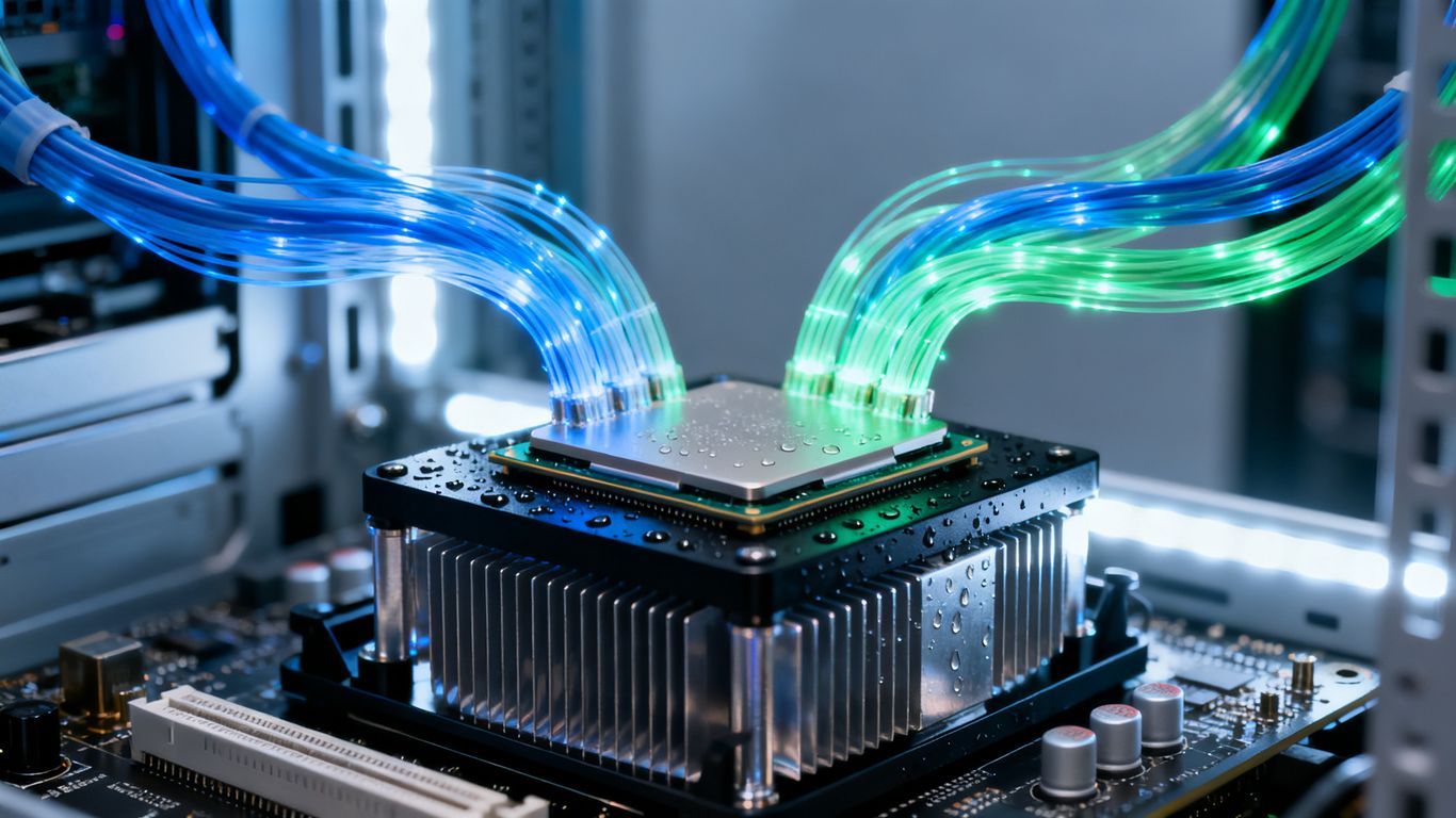
Co-packaging optics with processing units
Co-packaging shortens the length of the electrical trace from the chip to the converter, substantially reducing signal skew and power usage. This configuration necessitates advanced substrate design to ensure that the optoelectronic converter remains stable under the thermal duress of a high-performance processor.
Rethinking data center network topology
Traditional tree-like topologies are increasingly being replaced by flatter, more interconnected fabrics that facilitate lower-latency communication between any two points in the rack. Photonics acts as the physical layer that makes these complex, flattened topologies viable by removing the reach limitation of copper.
Future-proofing rack-scale AI systems
Building out a rack-scale system requires foresight regarding power requirements five years into the future. By moving toward a photonic quantum ready infrastructure, operators ensure that their network backbone will not require complete replacement as data throughput needs eventually move from terabytes to petabytes.
Current challenges and technical hurdles
Precision alignment of optical fibers and components
Achieving the sub-micron alignment precision required for laser-waveguide coupling represents a significant bottleneck for mass-market deployment. During the fabrication process, even minor mechanical shifts can lead to complete device failure or degraded performance.
- Advanced robotic assembly lines with micron-scale accuracy.
- Development of self-aligning structures on the chip substrate.
- Integration of thermal compensation materials for structural joints.
- Specialized housing to protect optical interfaces from vibration.
These strategies, while technically intensive, remain essential for ensuring that high-volume manufacturing remains feasible. Industry leaders are iterating on these processes to bring module assembly costs closer to parity with traditional electronic transceivers.
Reliability and thermal stability concerns
Lasers are inherently sensitive to temperature fluctuations, which risks shortening their operating lifespan within densely packed server racks. Designing packages that both dissipate high thermal loads from AI chips and protect the sensitive temperature-dependent laser components is a primary focus for infrastructure providers.
Standardization of pluggable and co-packaged optical interfaces
Lack of a universal standard slows the adoption rate across diverse vendor hardware. Without common interfaces for co-packaged optics, data centers remain locked into proprietary ecosystems that are difficult to scale.
Reducing the cost of high-volume photonic transceiver modules
Cost parity is the final hurdle for ubiquitous adoption. Significant investment in automated wafer testing and standardized packaging is allowing manufacturers to transition from bespoke enterprise deployments to general-purpose rack integration.
The future outlook for AI infrastructure
Development of full photonic compute engines
Research is shifting toward photonic-first compute engines that perform mathematical operations directly on the light signal before it is ever converted back into electrical form. This would essentially remove the energy-costly conversion steps, marking a massive leap for computational capabilities.
Impact on energy efficiency in exascale data centers
As data centers push toward exascale performance, the adoption of photonics becomes the primary method for maintaining an energy-neutral footprint. Reducing consumption by even a fraction of a percent across an exascale facility results in multi-megawatt savings annually.
Ecosystem collaboration and industry roadmaps
Industry roadmaps currently favor a gradual migration where optical links replace the longest distance electrical cables first. This phased transition permits Intel's focus on semiconductor-based advancements to support the broader ecosystem while developers refine the necessary manufacturing techniques for long-term viability.
The transition from copper to optical interconnects
Moving away from copper signifies a paradigm shift in how we build high-performance infrastructure for global intelligence. As standard signaling approaches its physical ceiling, the conversion to an optical backbone remains the only viable path forward for the next decade of development.
Conclusion
Silicon photonics stands as the foundational technology that will redefine how we build computing infrastructure for the artificial intelligence era. While significant technical hurdles in alignment and thermal management persist, the transition toward light-based networking is already underway, supported by innovations that allow us to bypass the physical limitations of current electrical standards. As these technologies mature, we can expect to see significantly more scalable and energy-efficient data centers, bridging the gap between current computation requirements and the massive demands of the next frontier.
Frequently Asked Questions
Why are traditional electrical cables insufficient for modern AI?
Electrical cables suffer from signal attenuation and heat dissipation issues that worsen significantly at higher data rates and longer distances, preventing the high-density throughput required for modern AI workloads.
What does co-packaging optics with processors mean?
Co-packaging involves housing the photonic optical engine and the computational processor on the same substrate or inside the same module, which dramatically shortens the electrical path between them and minimizes energy waste.
How does light make data centers more energy efficient?
Light transmission requires significantly less energy to move data across distances compared to copper, reducing the parasitic heat generation that dominates the cooling budgets in modern hyper-scale data centers.
Are there specific manufacturing challenges to silicon photonics?
Yes, the extreme sensitivity to laser-to-waveguide alignment and the requirement for precise thermal management are arguably the most difficult aspects of scaling photonic hardware for mass production.
Can silicon photonics work with existing server hardware?
Yes, the current industry approach involves bridging existing hardware architectures with photonic transceivers, often using pluggable architectures that function alongside legacy server designs before fully co-packaged solutions become mainstream.
How does this technology move beyond standard networking?
Beyond just signal transport, future research projects are exploring how to perform computations within the photonic domain, which would remove the need to convert data between electrical and optical formats repeatedly.
When will photonic computing be common in data centers?
While advanced photonic links are already appearing in high-end bespoke systems, the widespread integration of photonic interconnects into general-purpose data center racks is projected to accelerate over the next three to five years as standards mature.