Cerebras Wafer-Scale Engine, Reviewed: Breakthrough or Niche Bet?

Key Takeaways
The industry is observing a significant shift in AI hardware as large-scale silicon integration strategies challenge traditional GPU-heavy architectures, proving that purpose-built silicon can fundamentally change compute economics.
- Wafer-scale integration replaces hundreds of independent chips with a single monolithic processor fabric.
- Performance gains in AI training are primarily derived from reducing interconnect bottlenecks between cores.
- Software compatibility remains a hurdle, requiring mature compilers to map standard model architectures onto exotic silicon.
- Infrastructure efficiency is improved by consolidating power and cooling across a unified processor footprint.
- Economic viability depends on high-yield manufacturing processes coupled with specialized software stack support.
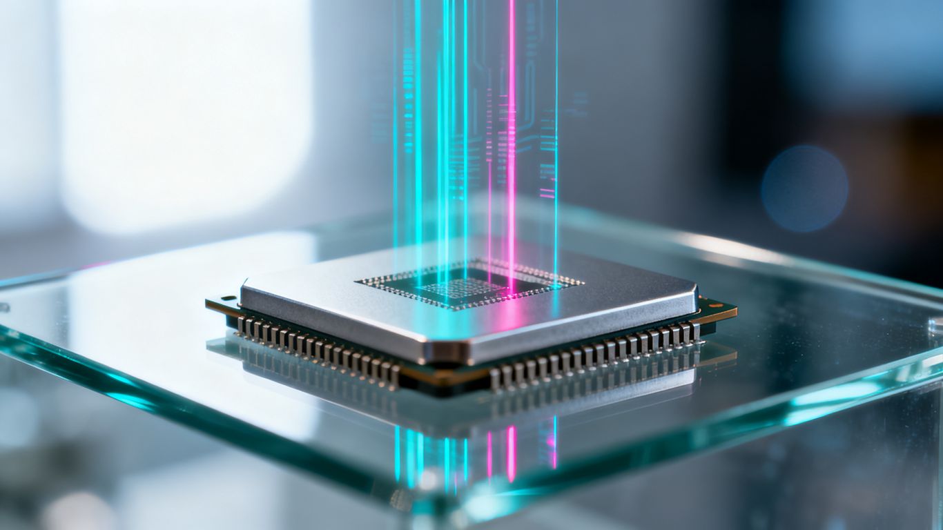
Understanding the Cerebras wafer scale engine architecture
The architectural shift toward wafer-scale computing represents a radical departure from the standard practice of dicing a wafer into individual dies. By keeping the wafer intact, the system preserves the massive bandwidth and connectivity inherent in the original silicon, which traditional cluster deployments often struggle to replicate without extensive networking overhead.
The shift to wafer-scale integration
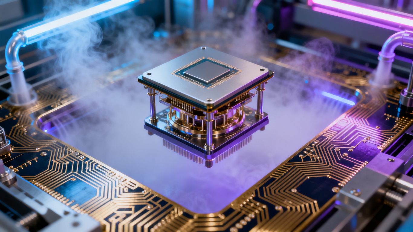
The internal design philosophy focuses on maximizing computational density by treating the entire semiconductor wafer as a single unit or processor. This approach minimizes the physical distance data must travel during complex machine learning tensor operations, essentially embedding the interconnect directly into the silicon itself for unparalleled speed.
Comparison with traditional GPU clusters
When we analyze Cerebras infrastructure, it becomes clear that moving away from high-density GPU racks changes how engineers deploy artificial intelligence inference engines. Traditional systems connect multiple independent chips through slow external interfaces, whereas this technology maintains a unified fabric that operates synchronously across millions of cores.
Interconnect density and memory bandwidth
Engineers often cite the massive local memory bandwidth available as the defining feature that allows for high-throughput computing. By keeping the static random-access memory directly adjacent to the compute cores, the system avoids the standard energy penalties and latency associated with moving data across a PCIe bus or InfiniBand network.
Performance metrics in real-world AI applications
Performance in actual production settings often exceeds the theoretical benchmarks typically seen in marketing materials, especially when workloads require heavy parallelization. This is where the hardware truly shows its potential, moving beyond simple chip specs into real-world model deployment metrics.
Training large language models
The ability to train massive models efficiently is largely limited by the speed at which gradients can be synchronized among processing elements. In this context, users typically track several key performance indicators to assess the utility of the architecture:
- Distributed weight update frequency during training
- Global synchronization latency for tensor parallel operations
- Total checkpoint throughput to non-volatile storage
- Effective utilization percentage per training epoch
These metrics demonstrate why users choose to move complex logic into this environment rather than sticking to conventional clusters.
Inference latency at scale
Inference latency is significantly reduced because the chip eliminates the need to traverse multiple network switches or local buses to reach high-speed memory. This allows for token generation rates that support complex, multi-stage reasoning tasks which would otherwise stall in slower environments.
Throughput for sparse computing workloads
Because the hardware is optimized to handle sparse computation patterns inherently, it achieves superior utilization on models that do not rely on dense matrix multiplication. This is particularly relevant for experimental architectures that utilize specialized gating mechanisms.
Software ecosystem and developer experience
Bridging the gap between exotic silicon and everyday deep learning frameworks remains the most significant barrier to broader adoption. Ensuring that popular libraries translate smoothly without requiring manual hardware-specific tuning is a critical focus for long-term platform viability.
The Cerebras software stack and compiler
The compiler serves as a critical translation layer, automatically mapping high-level code onto the physical silicon grid while managing data placement automatically. This abstraction is what allows the system to remain accessible to teams that do not employ dedicated semiconductor engineers.
Compatibility with standard frameworks like PyTorch
Native support for PyTorch is not just a feature but an essential requirement for most development teams working on generative AI workloads. By maintaining standard API compatibility, the hardware allows researchers to iterate rapidly without rewriting underlying model definitions.
Challenges in code optimization for non-standard silicon
Optimizing for non-standard silicon requires developers to re-think how they handle memory access patterns that might have been implicit on standard hardware. While high-level compilers hide this complexity, performance tuning often demands a deeper understanding of the underlying fabric.
Economic and infrastructure considerations
Infrastructure economics are reshaped when a user moves from an array of disparate processors to a single, monolithic unit that consolidates the entire compute fabric. This reduction in the physical data center footprint simplifies cooling and structural requirements significantly.
Power efficiency relative to traditional data centers
Comparing the power requirements of a single wafer-scale unit to a rack of GPUs reveals substantial differences in how heat is managed and energy is distributed across the compute fabric. The following table summarizes the comparative operational advantages often observed in high-density environments.
| Metric Category | Traditional GPU Rack | Wafer-Scale System |
|---|---|---|
| Power per FLOP | High | Low |
| Cooling Complexity | Distributed Exhaust | Integrated Liquid |
| Physical Floor Space | Multi-Rack | Single Cabin |
These factors collectively reduce the overhead costs that traditionally burden high-compute data centers as they scale.
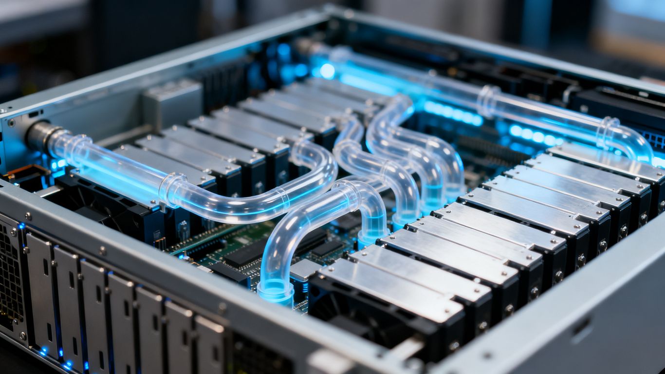
Physical footprint and cooling requirements
By centralizing the Cerebras Wafer Scale Engine, operators can utilize more efficient cooling configurations that do not require building-wide air circulation adjustments. This allows for higher density deployments in existing data center footprints that might otherwise be limited by heat dissipation capabilities.
Total cost of ownership for AI-first enterprises
Total cost of ownership is optimized not just by upfront hardware savings, but by the reduced technical debt in maintaining complex cluster networking. Enterprises focusing on AI inference speed often find that the operational simplicity is worth more than the acquisition cost as production cycles accelerate.
Advantages of the wafer-scale approach
The true value of a unified silicon architecture lies in its ability to erase the latency penalties normally incurred by crossing physical silicon boundaries, allowing for unprecedented speed in large-scale model training and inference.
This core philosophy guides every development decision regarding the hardware architecture, prioritize system-level performance over the isolated capabilities of single-process dies.
Reduced communication latency between compute cores
By placing all cores on the same silicon, the system achieves microsecond latency for inter-core communication, which provides a massive advantage for models that require frequent synchronization or complex, multi-modal reasoning capabilities.
Simplified cluster architecture management
Managing one piece of integrated hardware is fundamentally different than debugging a cluster of hundreds of GPUs. This reduction in system complexity allows the ops team to focus on model performance rather than network troubleshooting.
Scaling laws for next-generation generative AI
As models grow toward multi-trillion parameters, the interconnect bandwidth becomes the ultimate bottleneck. This approach to hardware ensures that compute capacity scales linearly with model size, avoiding the exponential costs associated with traditional networking layers.
Limitations and potential drawbacks
While the technology offers significant promise, it is not without risks that enterprise customers must consider before integrating it into production environments long-term.
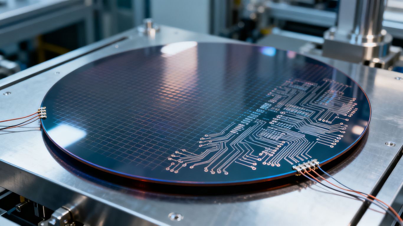
Manufacturing yield consistency and supply chain risks
Manufacturing silicon at this scale necessitates extreme precision, and defects are managed through redundant architecture rather than perfect photolithography. This creates a reliance on proprietary yields that may present long-term supply chain constraints compared to commodity chip production.
Potential for vendor lock-in
Selecting a hardware platform with an internal compiler stack often creates deep-seated dependencies on the manufacturer's specific roadmap. This makes it crucial for companies to evaluate the long-term support for software standards such as those found in CUDA alternatives to ensure that their models remain portable.
Versatility constraints compared to general-purpose GPUs
The optimization toward specificAI workflows ensures performance, but it may sacrifice the utility of the hardware in environments that require general-purpose computation or mixed-precision tasks that do not align with the chip's core routing logic.
Verdict: Defining the market for Cerebras
Positioning this technology within the broader AI hardware landscape requires a clear understanding of where the machine excels and where it remains specialized compared to established industry giants.
Ideal use cases for enterprise early adopters
Early adopters are typically enterprises building proprietary foundation models or high-throughput inference services that require lower latency than can be satisfied by standard cloud instances. For these teams, the system replaces massive infrastructure builds that would be significantly harder to calibrate.
Strategic positioning against market incumbents
Strategic positioning is maintained by focusing on the unique benefits of the wafer-scale integration path while addressing the integration hurdles that incumbents might solve through sheer scale. The company avoids head-to-head competition on commodity workloads in favor of niche high-intensity tasks where their architecture provides a clear multiplicative edge in speed.
Future outlook for the Wafer-Scale Engine iterations
Future iterations will likely focus on shrinking the feature size of the integrated nodes while increasing memory capacity to handle even larger parameter counts. As software compilers mature, the gap between custom silicon performance metrics and standard framework performance will narrow, further increasing the addressable market for these systems.
Conclusion
Advances in wafer-scale silicon demonstrate a clear path forward for entities requiring extreme throughput and lower latency than modular clusters provide. While software maturity and manufacturing yields remain key areas to watch, the structural advantages of a monolithic compute fabric offer a compelling alternative that redefines the deployment economics for large-scale generative models.
Frequently Asked Questions
How does unified silicon architecture differ from standard GPU clusters?
It removes the need for external network inter-device communication by embedding the fabric directly onto the wafer, which minimizes transmission latency.
Is the compiler compatibility a concern for existing model repositories?
Most modern models built on standard frameworks map reliably to the compute fabric, though custom layers might require specific attention during the compilation phase.
Can wafer-scale hardware be deployed in typical enterprise data centers?
Yes, though the unique cooling and rack-space requirements demand specialized facilities planning compared to standard blade-server environments.
What happens if a core defect is found on the wafer during manufacturing?
The architecture is designed to identify and isolate faulty nodes at the hardware level, allowing the remainder of the silicon to function normally without a drop in system availability.
Does this technology improve inference speeds for real-time applications?
By reducing the number of hops data makes between compute and memory, the system significantly decreases the latency per token, facilitating near-instant response speeds for complex queries.
Should startups focus on this platform early in their development cycle?
For teams focused on extreme latency requirements or proprietary large-model training, early adoption may provide a competitive advantage in performance throughput.
Is there a risk of being limited by proprietary hardware development?
As with any specialized silicon, there is always a consideration regarding vendor portability; companies often mitigate this by ensuring code portability at the framework level before committing to deployment.