Why HBM Memory Became the Real Bottleneck in AI
Key Takeaways
High Bandwidth Memory (HBM) has become the critical bottleneck in scaling artificial intelligence due to the massive data-transfer demands of modern neural networks.
- HBM uses vertical 3D-stacking to achieve bandwidths impossible for standard memory.
- The rise of large language models necessitates HBM's integration to prevent GPU starvation.
- Through-silicon via technology allows for massive data throughput within a compact silicon footprint.
- Supply chain complexity makes HBM a high-cost hardware component for hyperscale data centers.
- Future innovations like silicon photonics aim to overcome current limitations in inter-chip communication.
What is High Bandwidth Memory?
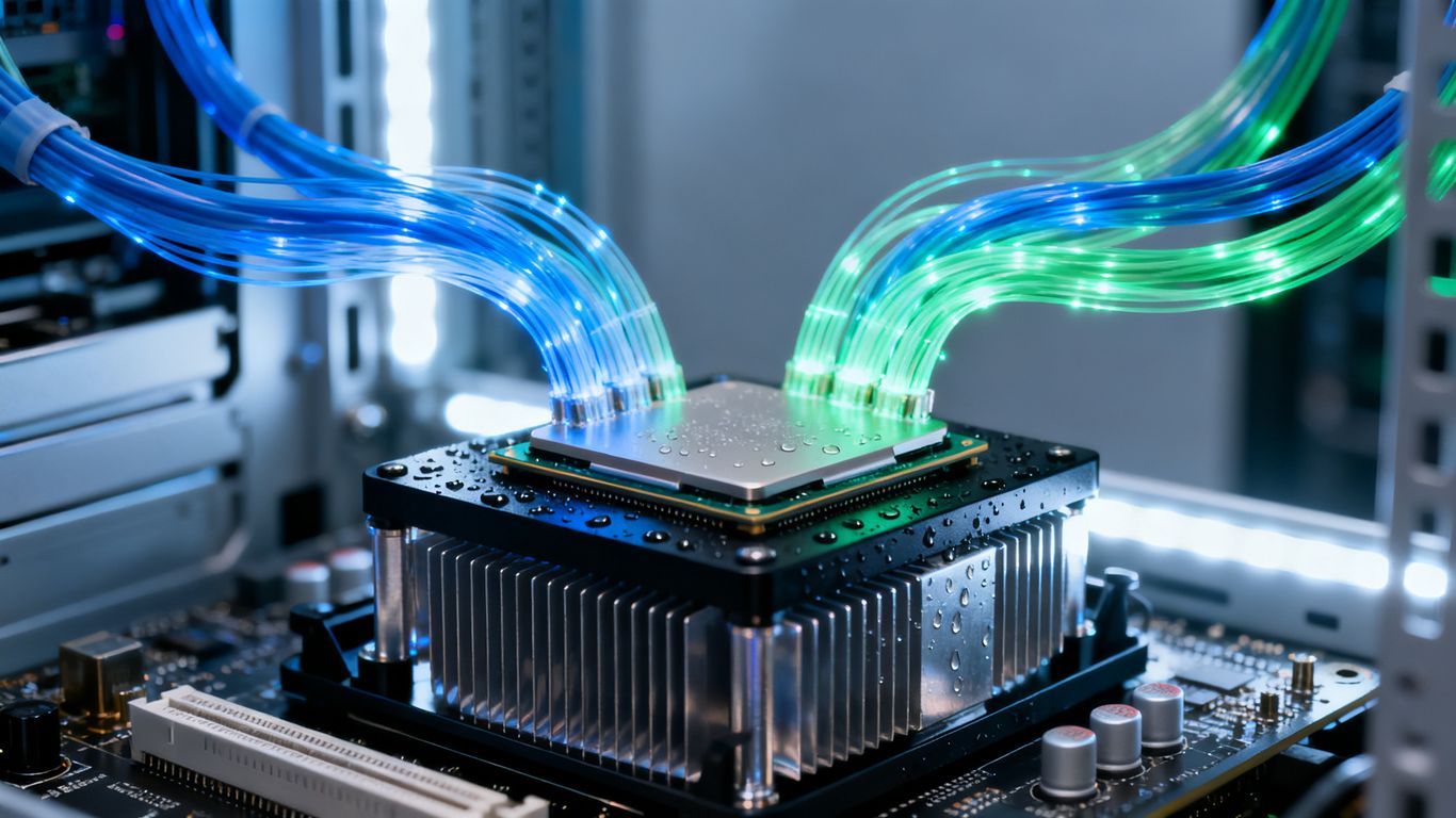
High Bandwidth Memory represents a significant shift from planar memory designs, focusing on maximizing data transfer speed within a thermal envelope that supports dense computing clusters. By stacking DRAM dies vertically, this architecture shortens the physical distance signals must travel. Inside Deep Tech researchers note that this design has fundamentally changed the memory hierarchy for modern accelerators.
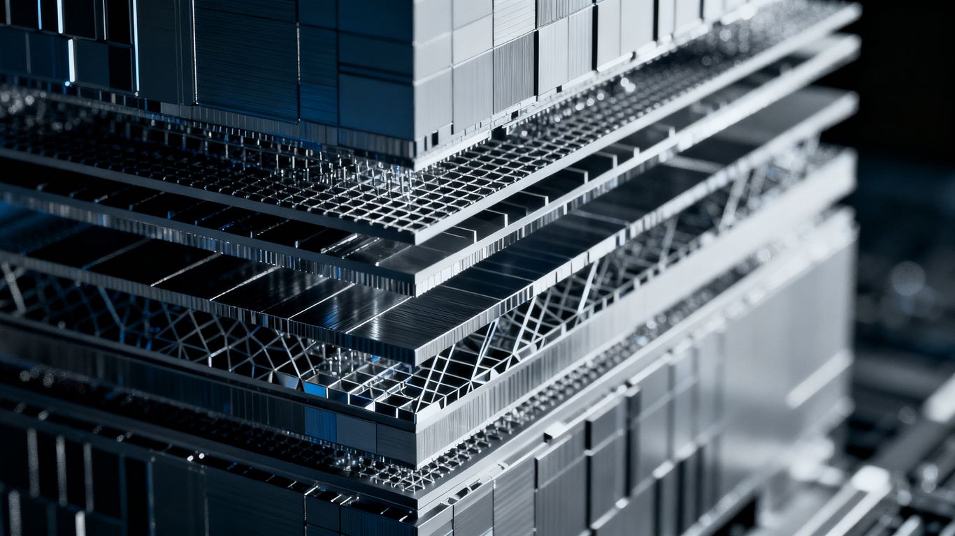
Defining the 3D-stacked architecture
The core of HBM lies in its vertical integration, where multiple memory layers are bonded together. This modular stacking approach allows for a vertical density that traditional layouts cannot reach, enabling complex 3D architecture designs that reside closer to the central processing unit.
How HBM differs from traditional DDR and GDDR
Unlike traditional DDR5 or GDDR6 memory that relies on wide, flat circuits across a motherboard, HBM utilizes an interposer to sit directly beside the processor. This architectural intimacy ensures that data paths remain short, minimizing the signal integrity issues common in legacy systems which often struggle with the sheer volume of tokens processed by modern generative AI workloads.
The role of TSV technology in vertical data transfer
Through-silicon vias (TSVs) serve as the electrical bridges between stacked memory dies. These tiny vertical connections provide a high-count pathway for data to flow from the stacks into the logic die. Without these low-latency conduits, the memory stacks would remain physically isolated from the intensive processing units they serve, rendering the bandwidth gains moot.
Why AI models create extreme memory demand

The shift toward complex neural networks has introduced requirements that exceed the memory capacity of previous compute generations. When training large language models, the requirement to swap parameters between storage and computation frequently creates a severe performance bottleneck. This phenomenon is known as the memory wall, and it forces engineers to fundamentally rethink hardware provisioning.
Parameters, weights, and the necessity of rapid data access
Modern large language models require constant access to billions of weights stored in memory. The speed at which these weights are retrieved determines the overall token generation rate of the system. Systems that cannot provide weight data fast enough effectively strand their expensive compute units during the inference phase.
Reducing inference latency in large language model training
To keep compute units active, system architects must prioritize memory bandwidth over total capacity in many specialized scenarios. Reducing the latency of these memory operations has become as important as increasing clock speeds for the processors themselves, especially when deploying models through services like AI inference chips platforms.
Throughput requirements in massive parallel processing
Parallel computing involves thousands of threads attempting to access memory simultaneously, which creates a highly contentious environment for data retrieval. Efficiently managing these demands requires a structured approach to hardware utilization. The following table outlines how different memory types handle these parallel stressors:
| Feature | GDDR6 | HBM3 | HBM3E |
|---|---|---|---|
| Data Path Width | Narrow | Ultra-Wide | Extreme |
| Power Efficiency | Moderate | High | Optimized |
| System Footprint | Large | Compact | Minimized |
These metrics demonstrate why HBM3 and its successors are essential for high-performance clusters. While legacy memory still serves lower-tier tasks, it often fails under the combined load of parallelized weight updates.
The technical link between HBM and performance
Memory bandwidth is the limiting factor for most advanced AI training runs today, often overshadowing compute capacity. By keeping memory chips physically proximate to the logic, hardware designers effectively mitigate the signal loss that occurs over long-distance traces. This proximity is why HBM is integral to current AI accelerators.
How bandwidth prevents GPU starvation
GPU starvation happens when a powerful chip sits idle because it lacks the data needed to perform mathematical operations. By providing a wider memory bus, HBM ensures that these chips operate near their theoretical maximum floating-point capacity. Inside Deep Tech recognizes that this specific link between throughput and utilization defines the next wave of infrastructure hardware.
Solving the physical limits of on-chip data transfer
As on-chip data transfer moves toward its physical limits, engineers are focusing on reducing power expenditure for every bit transferred. HBM achieves superior efficiency by moving smaller amounts of data over a massive number of parallel lines, rather than forcing high-frequency signals through a thin, power-hungry bottleneck.
Analyzing bottlenecks in current inter-chip communication standards
Inter-chip communication represents the next frontier, as data must often travel between separate physical stacks. These bottlenecks limit the potential for massive, unified memory pools where hundreds of chips operate on a single dataset. Current research into silicon photonics suggests that moving data with light rather than electricity could eventually solve this challenge.
Constraints in HBM production and availability

Manufacturing these high-performance memory devices is not a simple scaling exercise, as the precision required for TSV alignment is immense. The current supply chain for HBM is plagued by low yields on the most advanced node tiers, limiting global availability. Production is also hampered by the sheer complexity of testing 3D-stacked components before they are bonded to a processor.
The technical complexity of manufacturing HBM stacks
Manufacturing involves bonding layers of silicon with micron-scale accuracy, which inherently limits the speed at which wafers can be processed. Inside Deep Tech notes that this fabrication bottleneck forces long lead times for firms looking to upgrade their infrastructure, impacting everyone from major cloud providers to specialized inference-first hardware vendors.
The competitive impact of demand from major hardware firms
When major hardware firms consume the majority of available HBM, smaller players often find it impossible to procure these components at scale. This concentration of demand forces an industry-wide prioritization, where memory capacity is reserved for the most essential enterprise applications.
Economic barriers to scaling manufacturing capacity
Building out the required infrastructure for HBM production involves multi-billion dollar in capital expenditure. These economic barriers prevent rapid shifts in supply, meaning that market volatility remains a concern for project managers and financial strategists relying on consistent memory availability. To manage these risks, engineers often focus on the following strategies:
- Diversifying across primary silicon suppliers to stabilize inventory levels.
- Selecting architectures that support both current and legacy memory standards.
- Optimizing software code to minimize unnecessary memory throughput demands.
- Implementing hardware-level power management to extend the life of available memory modules.
These strategies help to insulate firms from the cyclical supply constraints that currently define the high-end memory market.
Why traditional memory architectures failed to keep pace
Traditional approaches, including GDDR6X, were built for graphical rendering pipelines where the data access pattern is predictable and consistent. In contrast, AI workloads are dynamic and largely unpredictable, stressing these legacy structures in ways they were never intended to handle.
The bandwidth limitations of GDDR6X for generative AI
GDDR6X suffers from physical trace limits that prevent it from achieving the sheer data throughput demanded by generative models. While perfectly capable of feeding frame-buffers for high-end rendering, it falls short when faced with the concurrent memory requests of an LLM.
The trade-off between power consumption and data access speeds
To extract higher bandwidth from a planar architecture, engineers often ramp up voltage and clock speeds, which leads to exponential power growth. HBM avoids this trap by using a wide interface, which delivers the same throughput at a fraction of the thermal cost.
Overcoming the memory wall in modern compute architectures
Breaking the memory wall requires a total reconfiguration of how computers handle data. This goal is driving the industry toward closer integration between processors and storage, and it remains a core pillar of the work described in various chipmaker reviews that assess modern system performance.
Innovations beyond current HBM standards
Industry progress is moving beyond simple bit-per-second metrics toward integrated compute-in-memory paradigms. These systems attempt to execute logic directly within the memory layer, eliminating the need to drag data across long silicon paths entirely. Such designs represent the next major evolution in data center architecture capacity.
Performance benchmarks of HBM3 and HBM3E
HBM3 and HBM3E represent the current state-of-the-art in usable memory throughput, offering doubling-per-generation performance gains. These tiers are already the industry standard for flagship AI compute modules, and they serve as the primary indicator for hardware competitiveness.
The potential of photonic and optical memory interconnects
Optical interconnects offer the ability to move data at the speed of light, effectively removing the distance-based bottlenecks of copper signalling. By utilizing lasers and waveguides, future memory systems will likely treat distant stacks as if they were sitting on the same local bus.
Designing for future memory-centric computing architectures
Designing for a post-HBM world means looking at universal memory pools, where the traditional distinction between CPU, GPU, and RAM disappears. This evolution is the logical conclusion for researchers aiming to build more efficient and powerful frontier AI systems that overcome the current memory-centric constraints.
Conclusion
High Bandwidth Memory is the linchpin of modern artificial intelligence, acting as the primary constraint on performance and scale. As the industry advances toward more complex 3D integration and eventually optical interconnects, the challenge will remain finding the perfect equilibrium between density, power, and throughput. Inside Deep Tech continues to monitor the intersection of memory science and silicon innovation as these technologies transition from laboratory prototypes to the foundation of the global compute landscape.
Frequently Asked Questions
What is the main cause of the memory wall in AI?
The memory wall occurs when the processor performs math faster than the memory can deliver data, causing compute units to wait in an idle state while waiting for information.
How does 3D stacking improve data throughput?
3D stacking allows memory dies to be placed in closer proximity to the processor, significantly shortening the distance electricity travels and enabling a larger physical interface between components.
What makes HBM more expensive than other memory?
HBM manufacturing involves delicate 3D packaging and alignment of TSVs across multiple silicon layers, creating lower yields and higher process complexity compared to traditional flat DRAM designs.
Why is thermal management critical for HBM?
Because HBM layers are stacked in a dense vertical assembly, heat dissipation becomes difficult; poor thermal management can lead to signal degradation or hardware failure within the device.
How do TSVs differ from standard memory wire traces?
TSVs are vertical shafts etched through the silicon substrate, meaning they can route data directly between layers of a stack rather than relying on lateral metal lines on the surface.
Are there alternatives to HBM for AI workloads?
While GDDR and SRAM are used for specialized compute tasks, HBM remains the standard for massive parallel AI workloads due to its unique combination of bandwidth density and power efficiency.
Will optical interconnects solve HBM bandwidth limits?
Optical interconnects are expected to remove the physical distance limits associated with copper communication, potentially allowing for much larger, geographically distributed memory clusters that function as one unified system.