
Key Takeaways
Photonic computing represents a fundamental shift in hardware architecture, utilizing light-based processing to bypass traditional electronic bottlenecks in AI infrastructure. By integrating optics directly onto silicon, industry leaders are addressing the thermal and bandwidth limits facing current high-end data centers.
- Photons provide significantly higher bandwidth density than electrons, enabling faster data transmission across chip architectures.
- Silicon photonics allows for the reuse of existing manufacturing nodes, potentially accelerating time-to-market for complex optical-electronic hybrids.
- Latency in large-scale model inference is reduced by direct optical matrix-vector multiplication, eliminating energy-intensive data conversion stages.
- Power efficiency gains in photonic systems are projected to support the continued scaling of deep learning models through 2026 and beyond.
- Current commercial viability depends on solving hybrid packaging challenges and establishing standardized design automation for mass-market deployment.
Understanding the fundamentals of photonic computing
The transition toward optical processing is driven by the physical limitations of electrical signals in modern hardware. As transistor density hits thermal ceilings, researchers are looking to light as a medium to carry information, which offers fundamental speed and efficiency benefits. Understanding this field requires a look at optical computing principles that differentiate it from standard von Neumann architecture, where processing and memory are often physically separated.
How light replaces electricity in data transfer
Unlike electricity, which travels through copper with resistance and parasitic capacitance, light moves through photonic circuits with minimal thermal loss. Data is encoded into the phase, amplitude, or wavelength of light waves, allowing for massive multiplexing that electricity cannot easily replicate.
The role of silicon photonics in modern hardware
Silicon photonics leverages established methods from the semiconductor industry to etch optical waveguides and modulators onto wafers. This approach enables the integration of optics directly onto the same die as high-speed controllers, creating a unified photonic integrated circuits pathway.
Key advantages over traditional CMOS technology
Photonic chips operate with lower signal degradation and provide near-instantaneous switching speeds for specific mathematical operations. By minimizing the heat generated during computation, these components allow systems to run at cooler, more stable temperatures compared to traditional transistors.
Distinguishing between optical interconnects and fully photonic processing
Optical interconnects act as a high-speed highway between chips, while fully photonic processing performs the calculation itself within the laser medium. The former is already scaling in data center racks, while the latter represents the long-term pursuit of computing with light waves rather than just moving data between electronic nodes.
Why photonics is critical for 2026 AI demands
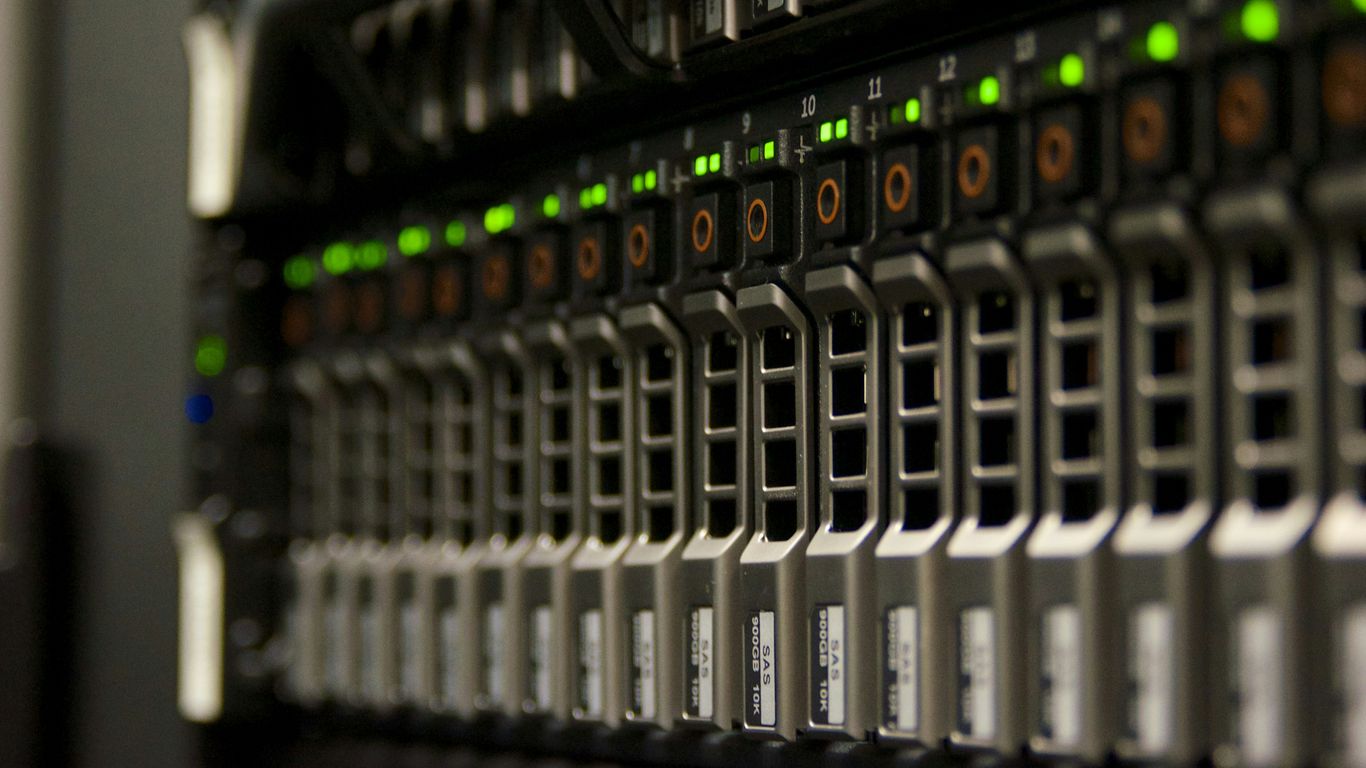
As AI model training grows, the dependency on traditional GPU clusters creates significant power walls that limit operational density. Photonics addresses these constraints by offloading intensive matrix calculations, which remain a primary driver of power consumption in current architectures.
Overcoming the power walls of current GPU clusters
High-power clusters rely on moving massive data sets between memory and processing cores, a task that consumes a disproportionate amount of energy. Implementing Passage® interconnects allows for lower energy per bit, alleviating the thermal strain on high-performance infrastructure.
Reducing latency in large language model inference
Standard inference often suffers from data-transfer bottlenecks that increase total response time for users. Photonic systems optimize these flows by allowing parallelized signal processing, which significantly decreases inference latency in large-scale model applications.
Addressing bandwidth bottlenecks in model training
Model training requires the constant exchange of gradient updates, a process that current electrical traces cannot support at scale. Photonics provides the high-bandwidth throughput necessary for effective synchronization, as demonstrated in these architectural components:
- Dense Wavelength Division Multiplexing to multiply signal capacity.
- Co-packaged optics that reduce the physical distance between processors.
- Low-loss waveguides that ensure signal clarity over longer chip distances.
- Distributed laser sources to minimize photon path length.
Sustaining the exponential growth of deep learning parameters
To keep pace with the ongoing expansion of model weights, the industry must adopt architectures that separate communication from computation. Photonic chips enable this by scaling the capacity of the fabric linking compute nodes without a commensurate increase in energy consumption per operation.
Comparing light-based chips to traditional silicon
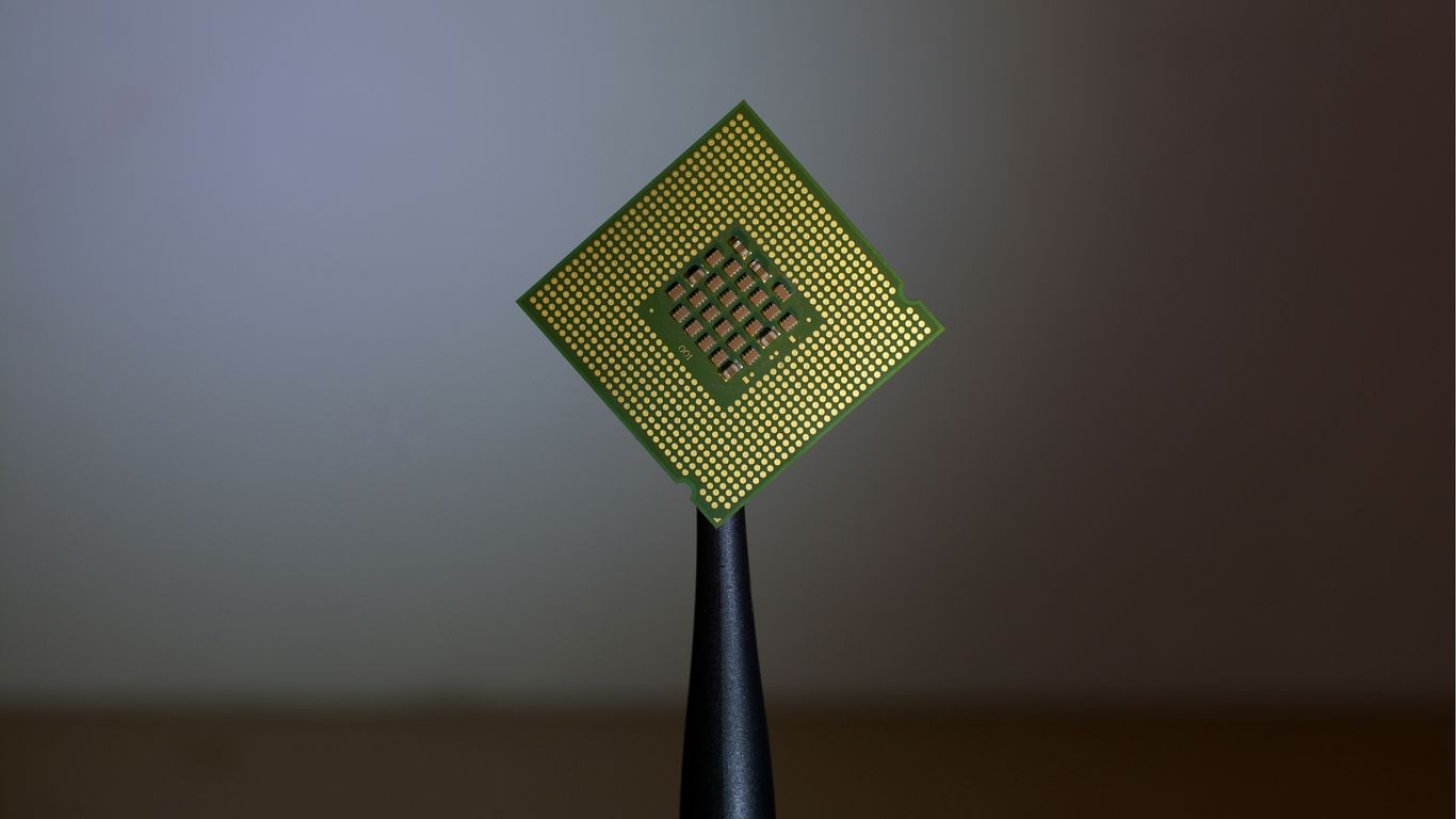
Choosing the right computational substrate requires balancing raw logic density against the physical realities of signal management and system heat. Modern AI chip landscape assessments frequently highlight how photons solve issues that electrical electrons struggle to address, ranging from EMI immunity to cross-talk between high-speed signal pathways.
Energy efficiency and chip thermal management
| Feature | Traditional Silicon | Photonic Processing |
|---|---|---|
| Signal Transmission | Electrical (Copper) | Optical (Photons) |
| Thermal Output | High (Heat generation) | Low (Minimal loss) |
| Processing Speed | Stagnant clock rates | Dynamic frequency scaling |
Throughput differences in parallel matrix processing
Parallel matrix processing is the backbone of deep learning, and photonic chips excel here by performing vector-matrix operations simultaneously across optical paths. This inherent parallelism allows for high-throughput calculation of dense parameter sets with fewer physical constraints.
Signal integrity and immunity to electromagnetic interference
Light waves are essentially immune to the electromagnetic interference that plagues high-frequency copper signaling. This robust signal integrity allows engineers to pack optical circuits closer together without the risk of crosstalk, facilitating denser high-speed connectivity.
Trade-offs between computational precision and raw speed
While traditional silicon offers extremely high precision for general-purpose tasks, photonic processors favor raw throughput for specific matrix operations. Engineers must often trade bits of precision for the speed that photonic acceleration delivers in massive, parallel deep learning workloads.
Core components of a photonic processing unit

Developing a functional photonic processing unit requires precise, nanometer-level control over how light interacts with semiconducting materials. Establishing a reliable hardware platform involves complex integration strategies that bridge the gap between pure research and commercial semiconductor mass production.
On-chip laser sources and integration challenges
Creating a monolithic light source on a silicon wafer remains one of the toughest challenges, as silicon is an inefficient light emitter at room temperature. Developers are currently using heterogenous integration to combine III-V materials with silicon, ensuring that laser emission remains stable and compact.
Mach-Zehnder interferometers for high-speed calculation
Mach-Zehnder interferometers serve as the fundamental switches for optical logic by manipulating the phase of light through split and recombine pathways. These components enable the execution of complex mathematical functions at the speed of light, essential for high-frequency matrix computation.
Photodetectors and analog-to-digital signal conversion
The efficiency of an entire computing system is only as high as its slowest conversion stage. As optical signals become the carrier for mathematical data, the translation back into electrical domains must be handled by high-sensitivity photodetectors to ensure systemic accuracy.
Optical waveguides and nanophotonic structures
Waveguides are the silicon-based conduits that guide light precisely where it needs to travel across a chip. Advanced nanophotonic structures allow for extremely tight bending radii, enabling engineers to create highly compact and efficient signal routing even in systems with high-density component placements.
Current barriers to mass commercialization
Scaling photonic technology entails meeting the rigorous quality and cost standards set by current large-foundry manufacturing models. The industry is currently working on specialized packaging that can move beyond experimental benches and into rack-stable infrastructure, ensuring that high-performance chips remain functional over years of sustained operation.
Scaling manufacturing for existing silicon foundries
Silicon foundries were originally optimized for electric transistor physics, not the fine manipulation of light modulators. Adjusting fabrication flows to include photonic specific materials ensures that optical components can be produced with the same high yields as classic processors.
Maintaining thermal stability in high-density circuits
High-density circuits create localized hot spots that can cause refractive index shifts in optical components, potentially de-tuning the system. Maintaining perfect thermal stability requires innovative cooling solutions integrated directly into the photonic substrate structure.
The complexity of hybrid electronic-photonic packaging
Packaging remains a significant hurdle because optical fibers must be aligned with extreme precision to silicon waveguides. Innovations in advanced semiconductor packaging are focusing on passive alignment techniques that simplify this procedure for mass-volume assembly lines.
Standardizing electronic design automation for photonics
Development today relies on fragmented or custom software models rather than a universal platform. Standardizing these tools is necessary for engineers to move from prototype development to rapid, verified layout production that silicon manufacturers can trust.
The competitive landscape of the AI hardware race
Investment is pouring into semiconductor startup incubators that demonstrate how specialized architectures for AI can lead the next phase of computing. These companies are navigating a shifting landscape where government-backed chip strategy and private-sector partnerships prioritize resilience alongside speed.
Strategic investments from major semiconductor incumbents
Major players are buying into the photonic ecosystem to secure future supply chains against shortages. By integrating internal research with strategic acquisitions, incumbents are creating comprehensive roadmaps that bridge the gap between legacy electrical infrastructure and future optical requirements.
The rise of specialized startups in photonic acceleration
Startups have become the primary drivers of innovation in this space, often focusing on niche but critical areas like neuromorphic computing or ultra-low-latency interconnects. These smaller firms allow for the rapid iteration of experimental materials like exciton-polariton quasiparticles before moving them into standardized production.
Government funding and national chip strategy alignment
National investments ensure that sovereign capability in advanced computing remains protected. By aligning private industrial goals with public policy, countries are creating a stable substrate of academic research and workforce training that supports the long-term feasibility of photonic infrastructure.
Prototyping progress and early industry partnerships
Early adopters in the cloud computing space are already running pilot programs using prototype photonic links in their infrastructure. These real-world deployments are invaluable for gathering telemetry on how optical hardware performs when scaled to thousands of nodes, proving the efficiency generational progress expects from next-generation systems.
Conclusion
Photonic computing is shifting rapidly from a laboratory interest to an infrastructure requirement as the thermal limits of traditional electrical circuits force a departure from monolithic designs. While manufacturing scale-up and standardization of design workflows present distinct challenges, the shift toward light-based processing offers the only reliable pathway to sustaining the current trajectory of deep learning hardware performance.
Frequently Asked Questions
Does photonic computing replace electrical computers?
Photonic computing is generally viewed as a complement to existing electronics, creating hybrid systems where light handles high-bandwidth and calculation tasks while electronics manage control and memory handling.
Why is heat a problem for current AI chips?
As transistor counts per area increase, resistance creates significant thermal output, which limits how fast and how densely these components can operate without compromising the stability of the system.
What are the main materials used in photonic chips?
Most current photonic chips are built on silicon, utilizing materials like silicon-on-insulator or added III-V materials to provide the necessary optical properties for lasers and modulators.
How soon will consumers see photonic processors?
Before consumer devices reach the hands of general users, photonic processing will likely be fully integrated into large-scale enterprise data centers to serve as an infrastructure backbone for cloud-native AI.
Does photonic computing work for all types of software?
Photonic systems excel at linear algebra and massive parallel matrix operations, which are the main workload of AI, but they are not currently designed to replace the general-purpose CPUs found in common home PCs.
What is the biggest barrier to photonic hardware today?
Scaling manufacturing for mass production, especially the high-precision packaging of optical fibers to chips, remains the most significant remaining constraint for wide-scale industry adoption.
Are there risks involved in optical data processing?
Outside of technical performance, the security of optical data transmission is a primary area of research, as the susceptibility of photonic circuits to physical tampering is different from standard electronic signal protection.