
Key Takeaways
Photonic computing represents a significant shift from electrical systems by utilizing light to process data, offering potential gains in bandwidth and energy efficiency. This article details the transition from traditional silicon circuits to light-based hardware architecture.
- Photons provide a massive increase in bandwidth through multiplexing techniques compared to electrons.
- Integration into existing electronic circuits creates energy-efficient hybrid systems for specific tasks.
- Thermal constraints in traditional silicon chips limit further miniaturization and clock speed improvements.
- Future adoption hinges on improving material science for optical components and manufacturing scalability.
- Photonic processors hold distinct advantages for accelerating high-frequency machine learning and AI workloads.
Fundamental principles of photonic computing
Wave-particle duality in information processing
Computational systems based on photonics harness the fundamental nature of light to encode information. By treating light as a wave, engineers utilize interference patterns to perform complex mathematical calculations natively without the binary step-wise processing required by silicon transistors.
Role of photons versus electrons in circuits
Unlike electrons that struggle with electrical resistance and heat, photons travel through waveguides with minimal attenuation. This inherent efficiency allows for higher clock speeds while maintaining a lower temperature profile within the device architecture.
Modulation and detection of light signals
Converting informational streams into optical pulses requires precise modulation of laser inputs. At the output, specialized sensors detect these signals, transforming the light back into accessible data states that electronic controllers can interpret for further processing or storage.
Comparison between electronic and photonic architectures
Energy dissipation in traditional silicon chips
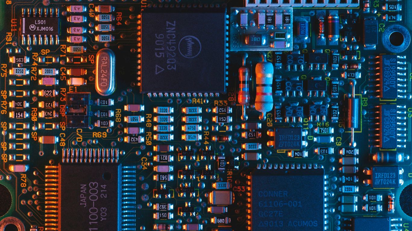
Traditional architecture suffers from heavy energy loss due to ohmic resistance in copper interconnects. As silicon geometry shrinks, the power required to drive these connections becomes a bottleneck, leading to thermal throttling and reduced overall performance.
Bandwidth advantages of multi-wavelength multiplexing
Light-based systems utilize wavelength-division multiplexing to send distinct data streams over the same physical waveguide simultaneously. This capacity far exceeds the signaling capabilities of traditional electrical traces, which face severe crosstalk at high frequencies.
Latency differences in signal propagation
Signal propagation via light occurs at a fraction of the speed of light, effectively removing the propagation delay constraints found in electronic backplanes. The consistency of these paths allows for predictable data throughput, which is essential for Inside Deep Tech to track infrastructure developments. The following table summarizes the key operational differences between these two hardware approaches.
| Feature | Electronic Computing | Photonic Computing |
|---|---|---|
| Data Carrier | Electrons | Photons |
| Energy Loss | Moderate to High | Low |
| Bandwidth | Limited by Wiring | Extremely High |
| Thermal Heat | Significant | Minimal |
These engineering trade-offs underscore why photonic modules serve as specialized accelerators rather than universal replacements for traditional processor cores.
Advantages of light-based hardware

Reduced thermal footprint and cooling requirements
Photons produce negligible waste heat compared to moving electrons. This allows designers to pack more logic into smaller volumes without needing exotic liquid cooling, which remains a standard requirement for high-performance supercomputing clusters today.
Parallel processing capabilities of light beams
Because light waves can intersect without interference, optical systems perform matrix multiplication in a single pass. This property is highly advantageous for artificial neural networks, which rely on massive parallel multiplication operations to weight connections between neurons.
Elimination of electrical capacitance constraints
Electrical capacitance limits how fast signals can toggle in metallic interconnects. Photonic circuits bypass these transient effects because light does not induce charge build-up, allowing for steady-state data transfer at speeds unreachable by traditional metal-gate architectures.
Practical challenges and engineering bottlenecks

Miniaturization of optical components on chips
Integrating optical lasers and waveguides directly onto CMOS dies requires managing disparate material properties. Silicon is not naturally well-suited for light emission, which forces engineers to explore complex hetero-integration strategies that maintain reliability across commercial manufacturing runs.
Difficulties in light-to-electricity conversion
Transitions between the optical and electronic domains consume significant energy and time. Minimizing this overhead is currently one of the most critical a1bd issues facing developers who hope to integrate these systems into existing data centers effectively.
Material science hurdles for photonic circuits
Finding light-sensitive materials that exhibit robust non-linear refractive properties at low intensities remains an active research area. Industry progress is tracked in d1fe, which outlines the long-term milestones required to move beyond experimental research devices.
Targeted applications for photonic processors
Accelerating artificial intelligence and machine learning workloads
Deep learning models rely on constant matrix arithmetic that maps perfectly to optical architectures. By offloading these specific calculations to an optical coprocessor, the primary CPU can manage orchestration and memory access more efficiently.
High-frequency trading and financial modeling
Financial firms seek the absolute lowest latency for their high-speed modeling tools. Photonic correlators offer the ability to process serial data streams with speed-of-light propagation, providing a competitive edge in environments where microsecond variations translate into distinct financial outcomes.
Next-generation telecommunications networking
Optical hardware is currently fundamental to f42b, ensuring that high-capacity backend infrastructure can manage the growing global demand for connected devices. These systems facilitate the rapid data routing required to support modern dense high-speed network loads.
Future roadmap for photonic technology

Hybrid systems integrating optical and electronic components
Most near-term solutions involve hybrid integration where optical engines manage intensive data flows while existing silicon handles standard logic. These systems must navigate several specific development stages to prove their value in the industry:
- Prototyping individual monolithic optical components for low-power operation.
- Establishing a standardized CMOS-compatible manufacturing flow for mass production.
- Optimizing software stacks to recognize and offload specific operations to photonic hardware.
- Realizing fully fault-tolerant optical-electronic interconnects at the rack scale.
This multi-step path defines how photonic technology will eventually become a ubiquitous feature of modern cloud architectures.
Transitioning from research labs to commercial manufacturing
Scaling from custom lab setups to automated foundry fabrication is the primary hurdle for venture-backed teams. Success requires moving away from manual optical alignment toward self-aligning wafer-level processes that mirror traditional semiconductor lithography.
Expected timelines for industry adoption
Industry experts suggest that niche enterprise applications will see deployments within the next 3-5 years. Broader consumer-side integration remains a much longer-term prospect, dependent on the maturity of 9501 frameworks that define standard performance metrics for hardware evaluation.
Conclusion
The trajectory of photonic hardware reflects a maturing field moving from academic curiosity to specialized industrial necessity. By addressing the fundamental physical limitations of electronic processing, light-based systems provide a clear path forward for the next generation of artificial intelligence and high-speed networking, promising a future where data density is no longer hindered by copper interconnects.
Frequently Asked Questions
How does photonic computing differ from modern silicon electronics?
Photonic systems use light waves to carry and process information, whereas silicon systems use electrons moving through solid-state transistors.
Is photonics intended to replace all electronic processors?
No, photonics acts as an accelerator for specialized mathematical tasks like matrix arithmetic, while electronic circuits will likely remain the primary choice for general-purpose logic.
What are the main obstacles to widespread adoption?
Key challenges include the complexity of manufacturing light-compatible materials alongside silicon and the energy cost associated with converting data between optical and electrical signals.
Why does light-based computing save on energy costs?
Light travels without electrical resistance, which eliminates the heat generated by electrical current moving through metal wires.
Can photonic computers operate at room temperature?
Yes, current development efforts focus on ensuring that optical chips can maintain performance without requiring cryogenic cooling, unlike some other emerging computing technologies.
Does photonic computing require new programming languages?
It generally requires optimized libraries and compilers that can interface with the optical hardware, rather than entirely new programming paradigms for the user.
What industries will benefit most in the near term?
Companies involved in high-frequency trading, massive neural network training, and telecommunications infrastructure represent the most likely early adopters due to their demand for speed.