Key Takeaways
The semiconductor industry is currently undergoing a structural shift toward specialized architectures designed to optimize AI workloads, moving well beyond traditional general-purpose processors. The following developments highlight the innovation driving this transition:
- Companies are increasingly adopting modular, chiplet-based designs to bypass the scaling limitations of monolithic silicon.
- Memory-centric architectures aim to solve the compute wall by minimizing data movement between memory and processing units.
- Optical interconnects are emerging as a viable solution for increasing throughput in massive-scale AI infrastructure.
- The rise of domain-specific silicon is challenging traditional dominance, offering alternative paths to achieving performance gains.
- Strategic partnerships and integrated software ecosystems remain critical factors for the successful deployment of custom AI hardware.
1. Tenstorrent
Tenstorrent has positioned itself as an architect of high-performance silicon, focusing on scale-out acceleration through its unique RISC-V based strategy. By emphasizing flexible, modular hardware design, the company seeks to address the evolving requirements of modern AI models and deep learning applications. Their approach centers on providing builders with the compute parity needed for complex neural network training and inference tasks.
As the industry explores options for AI chip companies, Tenstorrent separates itself by maintaining a hardware-agnostic software stack that can be ported across diverse architectures. This flexibility allows operators to scale their compute resources while managing the underlying infrastructure complexity. Their focus remains on enabling developers to move beyond fixed-purpose chips, providing a clearer path to deploying large-scale models.
The company’s roadmap emphasizes the importance of democratizing access to high-end silicon. By leveraging open standards and custom hardware, they are building tools aimed at future-proofing data center investments. This focus on long-term hardware compatibility aligns with current trends in AI infrastructure development, where shifting workloads demand adaptability at every functional layer.
2. Groq
Groq has effectively established its presence in the market by prioritizing deterministic latency for large language model inference. Their architecture replaces traditional buffer-based scheduling with a software-defined hardware approach that optimizes signal flow and resource allocation. This focus allows for high-throughput responses that avoid the bottlenecks common in standard processor designs.
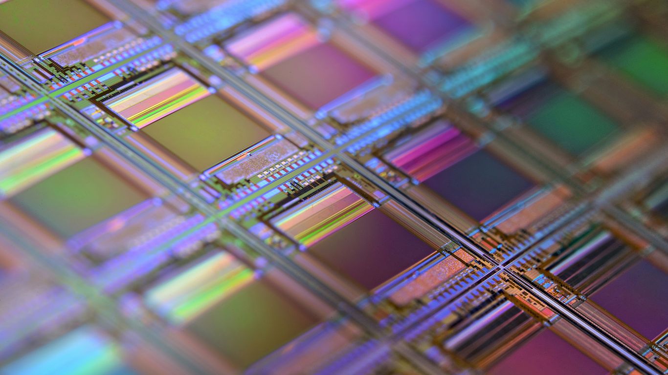
By keeping the hardware design simple and efficient, the company aims to reduce the jitter that often results from complex memory management. Their LPU (Language Processing Unit) serves as a testament to the benefits of removing legacy baggage from silicon architecture. It represents one notable example of how engineering decisions can drive significantly different performance profiles for real-time model interaction.
Looking at the broader impact on the industry, their specialized design serves as a case study for companies looking to optimize performance without sacrificing power efficiency. The focus on deterministic execution provides a blueprint for future infrastructure projects where predictable response times are a requirement. By targeting inference rather than massive-scale training, they address a specific niche in the market that is becoming increasingly critical.
3. Cerebras Systems
Cerebras Systems challenges the convention of traditional chip manufacturing by utilizing wafer-scale integration. By scaling a single chip across the entire surface of a wafer, they eliminate the need for traditional communication between multiple discrete GPU units. This physical consolidation simplifies the interconnection challenges that typically slow down massive multi-node training efforts.
This approach directly tackles the complexity of managing large-scale models that often span hundreds or thousands of nodes. By treating the entire wafer as one massive compute engine, the company provides researchers with a novel way to accelerate model runtimes. The resulting hardware has proven useful for academic and commercial institutions focused on high-performance compute tasks that cannot be easily parallelized.
Their innovation path highlights the tension between standard server architectures and extreme optimization approaches. While shifting toward massive monolithic silicon carries significant fabrication challenges, the benefit is a significantly reduced latency between cores. This move toward larger form factors indicates a shift in expectations for what deep tech hardware can achieve when freed from the constraints of commodity component standards.
4. SambaNova Systems
SambaNova Systems provides configurable hardware that adapts its data-flow execution to the specific software model being executed. By treating the underlying hardware as a software-defined fabric, they allow for a more efficient mapping of neural network structures onto their chips. This reconfigurable design ensures that computational power remains where the data needs it most.
Their focus on unified software ecosystems differentiates their offerings from those purely obsessed with raw clock speeds or peak operations per second. By lowering the barrier to entry, they help operators adapt to new model architectures without needing to undergo significant hardware refactoring. This approach serves as a critical enabler for companies looking to future-proof their internal AI initiatives.
As organizations search for the next generation of AI compute, they must weigh the benefits of specialized accelerators against the difficulty of software integration. SambaNova emphasizes that performance is only as good as the software's ability to utilize it efficiently. Their platform provides a balanced perspective on how modern silicon needs to bridge the gap between abstract research and actual production deployment.
5. Mythic
Mythic integrates analog computing directly into memory, which allows them to perform matrix multiplication tasks with significantly lower energy consumption than standard digital logic. This in-memory architecture is intended for peripheral edge systems where power budgets and heat dissipation are the primary constraints. Their design leverages the physical properties of flash memory to store weight values locally for inference processing.
| Feature | Benefit | Typical Use |
|---|---|---|
| In-memory Compute | Reduced Power | Edge Devices |
| Analog Logic | Low Latency | Real-time Vision |
| Integrated Scaling | Cost Efficiency | Passive Sensors |
This architectural shift is a departure from the power-hungry nature of general-purpose chips. The company’s focus on the edge brings intelligence closer to the data source rather than relying on backhaul to remote data centers. Consider an integrated, power-sensitive implementation:
- Minimizing data transport between memory and CPU.
- Enabling rapid inference for real-time image processing.
- Reducing dependence on external cloud connectivity.
- Facilitating long-term monitoring for remote infrastructure.
The most effective way to solve energy bottlenecks is to perform computation at the site of memory storage rather than moving bits across the chip for every cycle of calculation.
By keeping compute and storage adjacent, they bypass the traditional "von Neumann bottleneck" that plagues most silicon architectures. This approach is highly relevant for future projects using artificial intelligence in constrained, remote, or battery-powered contexts where efficiency dictates success.
6. Rain AI
Rain AI explores neuromorphic computing principles that mimic the synaptic density and interconnected nature of the human brain. Their approach focuses on creating hardware that can process information in a parallel, asynchronous manner, which stands in contrast to the rigid, stepped operations of traditional processors. By designing silicon that learns on its own hardware, they aim to reduce the energy overhead associated with training massive models.
This research into biomimetic hardware is becoming increasingly relevant as models scale in parameters and complexity. Their design targets a specific type of compute that favors high-density connectivity, allowing the chip itself to play a role in the learning process. Such advancements could fundamentally change the economics of building and maintaining large-scale intelligence.
The company’s roadmap is inherently long-term, moving beyond current benchmarks to address the underlying physics of deep neural networks. By reimagining the building blocks of a chip from first principles, they are exploring how architecture can match the efficiency of biological systems. This pursuit of fundamental structural shifts captures the interest of groups looking for long-horizon breakthroughs in silicon design.
7. Lightmatter
Lightmatter is pushing the boundaries of throughput by using photons instead of electrons to facilitate data movement and matrix calculations within the chip. By utilizing light, they can achieve a bandwidth density that is practically unreachable using standard copper-based interconnects. This optical approach aims to reduce heat and power consumption while increasing the speed of computation at scale.

Their modular optical architecture could redefine rack-level performance in massive data centers. By offloading inter-chip communication to light, they allow compute nodes to talk and share resources without the latency penalties usually incurred by massive overhead. This represents one of the most promising avenues for scaling infrastructure for future climate modelling, medicine, or advanced simulation.
Innovation in photonics is not just a leap in speed; it is an effort to fundamentally reconsider how nodes connect in a compute cluster. As structured data volumes continue to grow, the ability to pack more networking and compute capability into the same cabinet will become a defining differentiator for the dominant platforms. Their success could eventually influence how all large-scale accelerated computing systems are organized.
8. Untether AI
Untether AI creates at-memory compute architectures that move the calculation process directly into the SRAM arrays. By eliminating the distance that data must travel between memory banks and the processing logic, they drastically improve the energy efficiency of inference tasks. Their programmable hardware is designed to handle high-bandwidth needs while staying within a minimal power envelope.
This efficiency gain is a significant advantage for users processing large amounts of inference data in stationary environments like local area networks or autonomous hubs. By focusing on inference performance and energy-to-operation ratios, they offer potential for organizations that need to scale their analytics without incurring prohibitive utility costs.
Their architecture is built for ease of integration into existing systems, allowing companies as deep tech companies to incorporate specialized silicon without a complete, top-to-bottom redesign of their infrastructure. Whether in image recognition or text processing, the ability to maintain consistent throughput at lower power is a major advantage for practical, sustainable AI growth in the coming years.
9. Eliyan
Eliyan focuses on the chip-to-chip connectivity layer, specifically improving the bandwidth and power efficiency of data movement between disaggregated chiplets. As the industry moves toward complex system-on-chip architectures, the ability to connect various processing tiles seamlessly is critical. They provide advanced packaging and link technology that scales beyond traditional constraints of bandwidth per unit of surface area.
Their solution helps founders and system designers break up their monolithic silicon into manageable, specialized chiplets that communicate at high speeds but low energy cost. By enabling denser and faster interconnects, they facilitate the development of larger chips that would otherwise be rejected during fabrication due to physical limitations or yield issues. This focus on the "plumbing" of silicon is vital for the continued progression of massive computing hardware.
By making modular silicon a viable reality for small-to-mid-sized enterprises, they reduce the barrier for creating custom accelerators. This democratization of the interconnect layer allows designers to source heterogeneous silicon from different foundries, a trend that is becoming a reality in scaling global infrastructure for the long-term.
10. Celestial AI
Celestial AI creates optical communication fabric solutions that sit between memory and processing units. By separating the two, they allow for a disaggregated design where compute and memory can be scaled independently of one another. Their optical interconnect is designed to provide massive bandwidth that doesn't limit the efficiency of today’s powerful processors.
This separation is critical because it solves the capacity limits of memory on the chip itself. By enabling a flexible, high-speed connection between remote pools of memory and local accelerators, they provide a path to larger models that would not fit into the limited capacity found on single GPU boards. This approach helps in building more efficient server architectures for large language models and other memory-intensive applications.
Their technology represents the future of data-centric hardware architecture. By focusing on the movement of data between memory and silicon, they address one of the primary constraints of current infrastructure designs. As benchmarks for AI performance increase, the ability to reliably move bits will likely prove just as important as the ability to calculate them.
Conclusion
The landscape of silicon innovation is rapidly evolving as companies move beyond general-purpose processors toward highly specialized architectures. From optical interconnects to in-memory compute and wafer-scale integration, these startups represent the cutting edge of efforts to solve the most pressing challenges in AI scaling, power efficiency, and data throughput. While each firm adopts a distinct technical approach, they share a common goal of pushing hardware capabilities further than ever before.
Frequently Asked Questions
Why is the industry moving toward specialized silicon?
General-purpose processors are increasingly unable to handle the intense performance and efficiency demands of modern AI models and deep learning without consuming prohibitive amounts of electricity.
What are the main benefits of in-memory computing?
In-memory computing minimizes the power lost when moving data between memory banks and computational logic, which is a major bottleneck in traditional computing architectures.
How does chiplet-based design help scaling?
Chiplets allow manufacturers to build larger, more functional chips by combining smaller, high-yield components, bypassing the physical size and cost limitations of monolithic manufacturing.
Why is bandwidth a critical metric for AI chips?
High bandwidth is essential for ensuring that massive AI models can access the data they require for training or inference without waiting for memory traffic to clear.
What role do optical interconnects play in computing?
Optical interconnects use light to transmit data at significantly higher speeds and lower energy costs than traditional copper electrical wires, enabling higher-density compute clusters.
How do researchers assess the viability of new silicon?
Viability is often measured by looking at a company’s performance per watt, software ecosystem compatibility, and realistic production and deployment roadmaps.
What are the main challenges for new chip startups?
The primary hurdles include finding partners for advanced fabrication, the massive costs of R&D, and the difficulty of convincing established markets to switch their underlying software ecosystems.