
Key Takeaways
The landscape of accelerator hardware is shifting from general-purpose utility to purpose-built, highly specialized silicon designed for specific AI workloads. This transition is not merely an industry trend but a structural necessity driven by the intense energy and memory demands of modern generative models.
- General-purpose GPUs are increasingly constrained by the performance-per-watt requirements of massive training clusters.
- Hyperscalers are vertically integrating by developing custom silicon to optimize for their internal software stacks.
- Memory bandwidth and interconnect speed have emerged as the primary bottlenecks for scaling large language models effectively.
- Specialized NPU architectures are gaining traction for inference tasks where low latency is critical to user experience.
- The semiconductor market is diversifying, with foundries and design enablers playing a more central role in hardware democratization.
The landscape of the AI semiconductor market
The limitations of general-purpose GPUs
While graphics processing units initially provided the raw throughput necessary for early deep learning, their lack of optimization for specific neural network operations creates significant overhead. These chips excel at parallel floating-point arithmetic, yet they often squander power on fixed-function logic units that remain idle during specialized tensor operations. Modern AI chip companies beyond nvidia are recognizing that massive parallelism is not sufficient when data movement and memory latency dictate the real-world performance of an LLM.
Factors driving demand for specialized NPU designs
Neural Processing Units (NPUs) bridge the performance gap by baking architectural support for matrix multiplication directly into the silicon. By eliminating redundant components, these designs achieve superior computational density. Many of these firms, such as NVIDIA, have set the baseline, but newer entrants are finding success by focusing on the specific data-flow patterns of transformer-based models rather than maintaining broad compatibility.
The role of supply chain diversity in hardware selection
Engineering teams are increasingly prioritizing resilience and access in their procurement strategies to mitigate the risks of single-vendor dependencies. This search for alternatives often leads firms to explore AI chip makers, which provide more flexible integration pathways for custom data center racks. A balanced supply chain strategy now heavily features the following architectural categories:
| Architecture | Primary Use Case | Scaling Efficiency |
|---|---|---|
| General GPU | Flexible Training | Moderate |
| Custom ASIC | Specific Workload | High |
| Edge NPU | Local Inference | Very High |
Diversity in hardware sourcing reduces long-term operational risk, and firms are now diversifying by adopting a mix of merchant silicon and custom-designed accelerators for their production environments.
Long-term trends in semiconductor fabrication technologies
As we approach the physical limits of traditional lithography, the industry is pivoting toward modular chiplet architectures and advanced packaging. These techniques allow for higher yield rates and more flexible die combinations, essentially bypassing some of the historical constraints imposed by monolithic die sizes. The shift toward structured data processing in silicon will define the next cycle of performance gains, as throughput is now fundamentally tethered to how efficiently we can route data between compute units.
Established tech giants challenging NVIDIA
Intel’s Gaudi accelerators and enterprise strategy
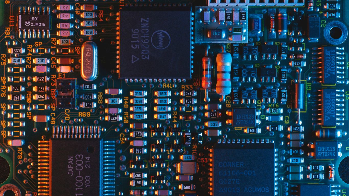
Intel focuses on providing a unified software experience that bridges the gap between traditional IT infrastructure and AI-specific compute requirements. Their strategy emphasizes the ease of migration for data centers using existing software stacks to handle complex training workloads.
AMD’s MI300 series and ecosystem competition
AMD has positioned its hardware as a direct competitor to high-end accelerators by emphasizing raw memory capacity and high-performance interconnect technologies. Their focus is on enabling large-scale model training while ensuring that developers can access a standardized programming environment that supports wide-scale model portability.
Broadcom’s role in custom silicon for large-scale data centers
Broadcom acts as a silent architect for the hyperscale world, designing the specialized ASICs that power internal data processing units inside the world’s largest server farms. Their core capability lies in developing high-speed networking and custom logic that enables massive hardware clusters to operate as a single logical entity.
Marvell’s focus on high-bandwidth optical interconnects
Marvell emphasizes the critical importance of low-latency data transport between compute nodes in a cluster. Because the speed of light—and the efficiency of photonics—eventually limits the scalability of training clusters, they have prioritized optical interconnect solutions that reduce power consumption while maintaining data integrity across distributed hardware setups.
Rising hyperscalers building custom silicon
Google’s TPU evolution and ecosystem integration
Google has built its entire AI research cycle around proprietary accelerators, creating a tight coupling between hardware and its own framework tools. By designing both the chip and the library, they ensure that every cycle is optimized for their specific mathematical workflows.
Amazon Web Services and the Trainium/Inferentia roadmap
AWS offers AI solutions through a managed roadmap that allows customers to swap between different classes of silicon based on their specific phase of development. Their strategy is centered on providing specialized units for both training and inference without requiring a full stack rewrite from the client.
Microsoft’s Maia AI accelerators for Azure internal workloads
Microsoft focuses its hardware efforts on optimizing performance for internal cloud-native workloads. Their approach treats hardware design as a software feature, iterating rapidly to match the architectural requirements of the large language models they deploy on their cloud infrastructure.
Meta’s strategy for proprietary inference hardware
Meta leverages proprietary silicon to handle the immense throughput requirements of their social media and generative AI applications. They prioritize energy efficiency for inference to manage the operational cost of serving models across millions of user interactions daily.
Emerging startups specializing in inference and edge AI
Cerebras Systems and the wafer-scale engine paradigm
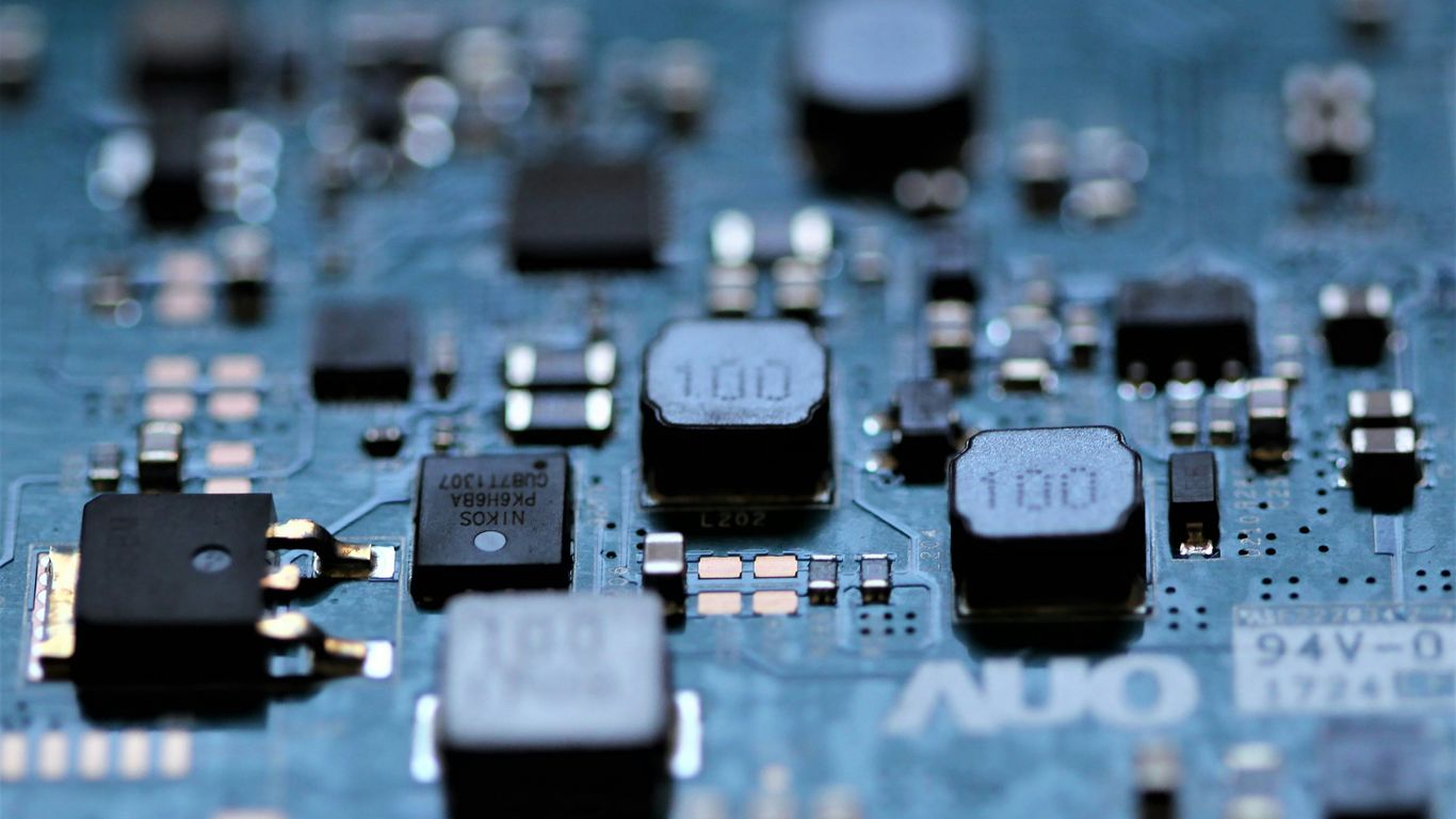
Cerebras Systems disrupts traditional packaging by utilizing an entire silicon wafer as a single compute unit. By minimizing the distance between memory and compute to the smallest possible physical extent, they avoid the overhead that typically plagues chips communicating across a printed circuit board. Their approach represents a fundamental shift in hardware strategy for developers managing dense model architectures.
Groq’s approach to low-latency language model inference
Groq designs hardware around a deterministic architecture that promises extremely low and consistent latency. By stripping away volatile scheduling layers found in traditional CPUs, their hardware ensures that each model generation step is predictable, which is essential for responsive LLM applications. They offer a distinct alternative for enterprises needing to integrate automated sales in real-time interfaces.
SambaNova Systems and end-to-end AI deployment
SambaNova Systems integrates physical hardware with a proprietary software layer, aiming to provide a seamless deployment experience for enterprise-scale foundation models. Their focus is on delivering a turnkey system that hides the complexity of underlying node-to-node memory transfers from the user.
Graphcore’s intelligence processing unit hardware
Graphcore designs chips that treat neural network graphs as the primary data structure for execution. Their hardware architecture allows for direct storage of model parameters within the compute node, which dramatically reduces the energy costs associated with frequent external memory access.
The impact of hardware architecture on AI scalability
Memory bandwidth as the primary bottleneck for LLMs
Inference performance is rarely limited by pure compute power, but rather by the speed at which data can be shuttled from memory banks to the processing logic. Architects are now building custom hardware that places high-speed memory physically closer to the processing cores to maximize effective utilization rates.
Balancing power efficiency with computational throughput
Efficient scaling in modern data centers is defined by the thermal envelope of the racks. When designing for the future, architects must weigh the benefits of exotic new transistors against the practical realities of electricity costs and physical cooling limitations.
Software stack maturity and developer accessibility
Building powerful hardware is insufficient if the tools are too difficult for researchers to use. Companies must provide robust compilers and intuitive diagnostic tools to ensure that developers can leverage the underlying silicon features without deep knowledge of low-level machine code.
The transition from training-focused to inference-optimized design
As the industry matures, there is an clear move from general training engines to dedicated inference chips. This specialization enables businesses to reduce the cost per token produced, essentially unlocking new AI applications that were previously too expensive to host in production environments. We can categorize this shift in the following ways:
- Move toward lower precision arithmetic to save power.
- Implementation of hardware-level support for sparsity.
- Increased reliance on on-die static memory buffers.
- Design shifts toward streaming data models.
This evolution ensures that hardware remains aligned with the changing needs of the production AI lifecycle.
Conclusion
The market for AI infrastructure is currently decoupling from a single-vendor hegemony, with specialized silicon becoming the primary way to achieve efficiency at scale. While giants continue to innovate on a massive scale, the diverse architectural bets placed by hyperscalers and agile startups ensure a robust future for compute technology. Investors and engineers who look toward this broader horizon will find that the next phase of deep tech will be built upon an increasingly heterogenous foundation where the software dictates the hardware form, and the architecture constantly adapts to meet the ever-climbing requirements of frontier research.
Frequently Asked Questions
What defines an application-specific integrated circuit in the context of AI?
An ASIC is designed for a single type of workload rather than having the wide-ranging general-purpose capabilities of a standard processor. This design philosophy allows the circuit to achieve higher efficiency and lower power consumption by removing unused logic components.
Why is memory bandwidth such a significant challenge for modern AI hardware?
Large language models operate by shuffling billions of parameters through a processor, and traditional memory speeds cannot always keep up with the execution units. When the processor waits for data from the memory, it idles, and efficient hardware must therefore minimize the distance and travel time between these two physical locations.
How does wafer-scale architecture differ from traditional chip design?
Traditional chips are cut from a wafer and then packaged into smaller units, whereas wafer-scale engines use one large, interconnected die for the entire calculation. This design reduces the need for off-chip communication, significantly lowering the bottlenecks associated with data transport.
Why are companies moving toward custom silicon for inference tasks?
Inference is often the most costly ongoing component of an AI service, especially as usage grows into the millions of requests. By building silicon specifically optimized for the inference pass, companies can reduce their energy usage and hardware volume, directly impacting their bottom line.
Are general-purpose GPUs becoming obsolete for large-scale training?
GPUs remain the industry standard due to their versatility and mature software ecosystem, meaning they are far from obsolete. However, they are increasingly being supplemented—and in some specific domains, challenged—by more specialized silicon designed for specific data flow patterns.
What role do optical interconnects play in high-performance computing?
Optical interconnects use light to transmit data, which allows for faster movement than copper wires over longer distances and with far less heat. This is becoming a critical component for large clusters where the overhead of moving data between distant cabinets is limiting the overall training speed.
How can hardware architecture enable more sustainable AI development?
Architecture impacts the energy required for every dollar of computation performed by a cluster. By moving from general-purpose hardware toward more efficient, task-specific circuits, researchers can perform more science and developers can host larger models for the same amount of electricity and cooling resources.