Most AI clusters still start with GPU shopping lists. That habit is rational. NVIDIA's CUDA stack, NVLink domains, and InfiniBand scale-out still define how most teams ship models. It is not the only high-volume path.
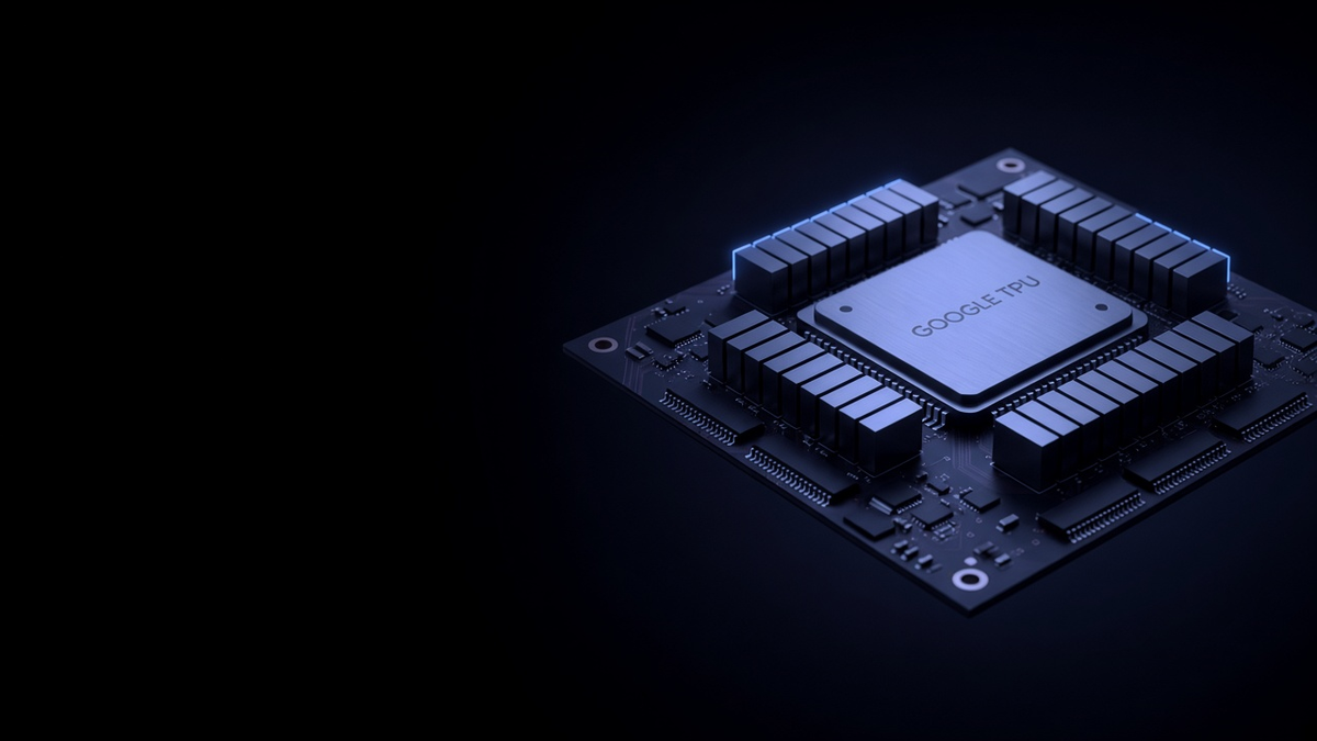
This guide covers Google's Tensor Processing Unit (TPU): the ASIC Google designs for matrix-heavy training and inference, ships in Cloud TPU Pods, and exposes through TPU VMs and slices. You will get the systolic-array architecture (MXU / TensorCore / SparseCore), the generations that matter as of September 2026 (v5p, Trillium/v6e, Ironwood/TPU7x), Pod and Slice networking over ICI, the JAX / XLA / PyTorch software path, when TPUs beat GPUs and when they lose, and an honest limits section. Specs below come from Google Cloud documentation and AWS Neuron docs, not invented datasheets.
Key Takeaways
- TPUs are Google ASICs built around systolic MXUs for dense matrix math, not general GPUs.
- As of September 2026, Ironwood (TPU7x) is GA with 2,307 BF16 TFLOPs and 192 GiB HBM per chip.
- Pods wire chips over ICI; you rent a Slice (topology) via TPU VMs, GKE, or Compute Engine.
- JAX and XLA are first-class; PyTorch/TorchTPU and vLLM paths exist, but CUDA gravity still wins many teams.
- TPUs win on Google-shaped batch training and Pod scale; they lose on CUDA lock-in, odd kernels, and scarce capacity.
What a Google TPU actually is
A Tensor Processing Unit is Google's application-specific integrated circuit for machine learning. Google Cloud's architecture docs are blunt: TPUs are matrix processors. They are not general-purpose CPUs, and they are not GPUs that happen to run GEMMs well. The chip spends silicon on multiply-accumulate arrays that stream operands through neighboring ALUs so matrix products do not bounce every intermediate result back to memory.
That pattern is a systolic array. Google's classic TPU blog and the current system-architecture page both describe the Matrix Multiply Unit (MXU) this way: load parameters into the array, stream activations, pass partial products to the next MAC, accumulate in FP32. Modern Cloud TPU MXUs use 256×256 multiply-accumulators on TPU v6e and TPU7x, and 128×128 on earlier generations, with bfloat16 multiplies and FP32 accumulation (Google Cloud TPU architecture docs, updated September 2026).
Each chip packages one or more TensorCores (MXU plus vector and scalar units) and, on recent generations, SparseCores that accelerate embedding gather/scatter for recommendation-style workloads. Ironwood (TPU7x) and v5p put four SparseCores on a chip; Trillium (v6e) puts two. That split matters when your model is dense Transformer math versus embedding-heavy ranking.
Architecture: MXU, memory tiers, and dual chiplets
Think of a modern TPU chip as three cooperating engines plus a memory hierarchy, not as a miniature GPU SM farm.
- MXU systolic array: the FLOPs factory for dense matmul. Tile sizes and batch shapes that keep the array fed win. Irregular control flow and tiny batches lose.
- Vector and scalar units: activations, norms, address math, and control that the MXU should not waste cycles on.
- SparseCore: dataflow path for large embedding tables and sparse ops, sharing the Pod's ICI fabric.
- HBM: the working set. Ironwood documents 192 GiB HBM per chip at about 7.38 TB/s. Trillium is 32 GiB at 1.638 TB/s. v5p is 95 GiB at 2.765 TB/s (Google Cloud comparison tables).
- On-chip VMEM / scratch: high-bandwidth SRAM near the MXU for custom kernels (Pallas/Mosaic on Ironwood). Host DRAM over PCIe is the overflow tier, not the happy path.
Ironwood adds a manufacturing and programming twist. Google Cloud's TPU7x page describes a dual-chiplet package: two chiplets, each with one TensorCore, two SparseCores, and 96 GiB HBM, linked by a die-to-die interface Google says is six times faster than a 1D ICI hop. Frameworks such as JAX expose two devices per physical chip. That is a break from the MegaCore unified-memory model on v4/v5p. Existing models mostly port, but topology specs gain a chiplet dimension and NUMA-aware host binding still matters on the 4-chip VM.
Memory pressure is still the day-to-day constraint. Large HBM helps batch size and KV cache, but vector-heavy or poorly tiled kernels stall on bandwidth. Inside Deep Tech's HBM full guide is the packaging and supply companion to this chip story: every serious accelerator, TPU included, is gated by stacked DRAM and assembly slots such as TSMC CoWoS.
Generations that matter in 2026: v5p, Trillium, Ironwood
Ignore marketing generation numbers for a moment and read the Google Cloud tables. As of September 2026, the shipping Cloud TPU lineup operators actually provision includes v5p, v6e (Trillium), and TPU7x (Ironwood). Older v4/v5e remain relevant for migration, but new large jobs center on these three.
| Spec (per chip unless noted) | v5p | v6e Trillium | TPU7x Ironwood |
|---|---|---|---|
| Chips per Pod | 8,960 | 256 | 9,216 |
| Peak BF16 TFLOPs | 459 | 918 | 2,307 |
| Peak FP8 TFLOPs | 459 | 918 | 4,614 |
| HBM capacity (GiB) | 95 | 32 | 192 |
| HBM bandwidth (GBps) | 2,765 | 1,638 | 7,380 |
| Bidirectional ICI (GBps) | 1,200 | 800 | 1,200 |
| TensorCores / SparseCores | 2 / 4 | 1 / 2 | 2 / 4 |
| Interconnect topology | 3D torus | 2D torus | 3D torus |
| 4-chip VM vCPU / RAM | 208 / 448 GB | 180 / 720 GB | 224 / 960 GB |
Source: Google Cloud documentation pages for TPU v5p, TPU v6e, and TPU7x (tables last updated around 18 September 2026). Trillium's product page also claims about 4.7× peak compute per chip versus v5e and 67% better energy efficiency versus that prior generation. Ironwood's product page claims 42.5 ExaFlops at Pod scale, liquid-cooled 9,216-chip Pods, and roughly 4× performance per chip versus Trillium.
How to read the table without fooling yourself:
- v5p: still the large 3D-torus training workhorse with nearly 9k chips per Pod and strong SparseCore count for embedding-heavy jobs.
- Trillium (v6e): smaller 256-chip Pod, 2D torus, lower HBM per chip, higher BF16 peak than v5p, strong inference and mid-scale training economics.
- Ironwood (TPU7x): GA seventh generation for dense and MoE training plus decode-heavy inference; dual chiplet; TensorFlow explicitly not supported on TPU7x per Google's TPU7x page (use JAX or PyTorch).
Google's marketing site also lists TPU 8t and TPU 8i as Coming soon (pre-training / embeddings versus post-training / inference). As of this writing they are not treated as generally available Cloud SKUs in the architecture docs you provision from.
Pods, Slices, TPU VMs, and ICI
Cloud TPU vocabulary is precise. Get it wrong and capacity tickets fail for stupid reasons.
- TPU Pod: the physical contiguous cluster of chips on Google's specialized fabric (thousands of chips on v5p/Ironwood; 256 on Trillium).
- Slice: the subset of a Pod you actually get, defined by a topology (for example 4x4x4 = 64 chips on Ironwood). Chips in a slice talk over Inter-Chip Interconnect (ICI).
- TPU VM: the Linux host with direct access to attached TPU chips (Ironwood: full-host 4-chip VMs with 224 vCPUs and 960 GB RAM).
- Multislice: multiple slices glued over the data-center network (DCN) when one ICI domain is not enough. Google documents Multislice primarily through GKE / Megascale XLA paths, not as a casual single-VM feature.
- Cube: a 4x4x4 building block for 3D topologies from v4 onward.
ICI is the TPU equivalent of NVLink inside a domain. Google Cloud quotes bidirectional ICI bandwidth of 1,200 GBps per chip on v5p and Ironwood, and 800 GBps on Trillium. Between cubes, optical paths and optical circuit switching show up in Google's published TPU v4 and later designs. That is why Inside Deep Tech's OCS full guide keeps referencing TPU Pods: Google already runs photonic circuit switching at Pod scale while GPU halls still argue copper versus CPO.
Access models as of September 2026:
- Compute Engine TPU VMs / MIGs for v5p, v6e, and TPU7x (with Multislice limitations called out in Google's Compute Engine TPU docs).
- GKE with accelerator topology for production scheduling, Multislice, and All Capacity mode reservations on Ironwood.
- Vertex AI managed training and prediction paths for teams that refuse to own node pools.
Host attach is still PCIe-class relative to HBM. That is fine for orchestration and offload. It is not your all-reduce fabric. For the GPU-side interconnect map, see NVLink, InfiniBand, and UALink and PCIe 6.0. TPU ICI owns the accelerator mesh; PCIe feeds hosts and peripherals.
Software: JAX, XLA, PyTorch, and the compiler tax
Hardware without a compiler story is a paperweight. Google's TPU stack is compiler-first.
- XLA (Accelerated Linear Algebra) lowers framework graphs into fused kernels that target MXU/VPU schedules.
- JAX is the research and large-scale training default: explicit meshes, pmap/pjit-style sharding, and first-class multi-host slices. Google ships MaxText and post-training libraries on this path.
- PyTorch on TPU (TorchTPU / eager-first stacks Google markets with Meta) reduces rewrite cost for CUDA-native teams, but you still compile hot paths and watch for op gaps.
- Pallas + Mosaic (highlighted in Google's Ironwood codesign blog) let experts tile HBM to VMEM deliberately when XLA's autotuning leaves FLOPs on the table.
- Inference: Google's product page calls out vLLM on TPU for high-throughput serving. Treat that as a supported direction, then verify the exact engine version for your generation.
Here's the problem. CUDA's gravity is not a benchmark score. It is fifteen years of kernels, profilers, vendor examples, and hiring funnels. A team with a custom FlashAttention variant, a weird MoE router, or a dependency on NVIDIA-only libraries will burn weeks before the first clean TPU step. JAX-native or carefully XLA-friendly PyTorch codebases convert faster. "We use PyTorch" alone is not a migration plan.
Ironwood's dual-chiplet exposure is another software detail buyers miss. Two devices per chip changes device counts, mesh axes, and how you reason about local HBM. Google documents that existing models need minimal changes, which is true until someone hard-codes assumptions from MegaCore generations.
When TPUs beat GPUs (and when they lose)
Buyers want a single winner. Reality is workload-shaped.
Where TPUs tend to win
- Large, stable matmul graphs with batch sizes that keep systolic arrays busy (foundation-model pre-training, dense Transformer blocks).
- Jobs that fit Google's Pod topology and Multislice story, especially when you already run on GCP and want ICI instead of assembling NVLink islands plus an InfiniBand fabric.
- Embedding-heavy recommenders that actually use SparseCore instead of pretending a GPU is an embedding appliance.
- Organizations standardized on JAX / XLA (or willing to be), including Google-internal-style MaxText training recipes.
Where GPUs (and other ASICs) tend to win
- CUDA-native codebases, custom Triton/CUDA kernels, and ecosystems that assume NVIDIA profilers and NCCL defaults.
- Highly dynamic shapes, experimental research ops, or frameworks with incomplete TPU lowering.
- Multi-cloud or on-prem strategies that need the same accelerator SKU everywhere. TPUs are a Google Cloud (and Google internal) product, not a merchant ASIC you buy in a whitebox.
- Teams that need the broadest third-party model zoo and ISV support tomorrow morning.
AWS Trainium2 is the cleanest hyperscaler peer for comparison: another custom train ASIC with its own Neuron compiler stack. Per AWS Neuron docs, a Trainium2 chip delivers 1,299 FP8 TFLOPS and 667 BF16/FP16/TF32 TFLOPS with 96 GiB HBM at about 2.9 TB/s, plus NeuronLink-v3 at 1.28 TB/s per chip. That is not an apples-to-apples bake-off against Ironwood's 4,614 FP8 / 2,307 BF16 TFLOPs and 192 GiB HBM, because instance topology, software maturity, and price/availability dominate. It is enough to show every hyperscaler is shipping non-GPU train silicon with compiler lock-in of its own.
| Dimension | Google TPU7x (Ironwood) | AWS Trainium2 | NVIDIA GPU cluster (typical) |
|---|---|---|---|
| Chip peak (sourced) | 2,307 BF16 / 4,614 FP8 TFLOPs; 192 GiB HBM (Google Cloud) | 667 BF16 / 1,299 FP8 TFLOPS; 96 GiB HBM (AWS Neuron) | Generation-specific; buy from NVIDIA datasheets for the SKU you run |
| Scale-up fabric | ICI inside Slice/Pod (1,200 GBps bidirectional/chip) | NeuronLink-v3 (1.28 TB/s/chip) | NVLink / NVLink-C2C domains; see IDT NVLink guide |
| Scale-out | DCN + Multislice; OCS inside Google Pods | EFA / UltraServer topologies on Trn2 | InfiniBand / RoCE / Ultra Ethernet |
| Primary software | JAX, XLA, PyTorch/TorchTPU; no TF on TPU7x | Neuron SDK, PyTorch/JAX via Neuron | CUDA, cuDNN, TensorRT, NCCL |
| Where you buy it | Google Cloud TPU VM / GKE / Vertex | AWS EC2 Trn2 / UltraServers | Cloud GPUs + on-prem OEM servers |
| Honest limit | Capacity, JAX/XLA fluency, Google-shaped ops | Neuron maturity vs CUDA breadth | Cost, power, and NVLink island size |
Gaudi, Cerebras, and Groq belong in the same buyer conversation as "custom silicon alternatives," but their public one-chip peak numbers change by SKU and marketing unit. Inside Deep Tech will not paste unsourced FLOPs into this table. Evaluate them on compiler maturity, memory model, and whether your model graph maps to their execution style.
Honest limits: lock-in, capacity, shapes, and cooling
Name the downsides before procurement does it for you.
- Ecosystem lock-in: TPUs run where Google operates them. You are buying into XLA semantics, Google Cloud networking, and Google's capacity map.
- CUDA gravity: hiring, examples, and third-party kernels still orbit NVIDIA. Budget rewrite and profiling time, not just chip-hours.
- Availability: large contiguous topologies are quota and reservation games. Spot and next-Tuesday 2,048-chip fantasies fail quietly.
- Batch and shape sensitivity: systolic arrays hate tiny batches, pathological padding, and host-bound preprocessing. Throughput cliffs are real.
- Framework gaps: Ironwood drops TensorFlow support per Google's TPU7x docs. Verify every custom op on your target generation.
- Dual-chiplet surprises: device counts and mesh axes change. Ports from MegaCore assumptions need a topology review.
- Facility load: liquid-cooled Pods at Ironwood scale are a power and water problem for any hall that hosts them.
For rack thermal reality, see data center liquid cooling. For chip-to-chip photonics that sits beside these Pods as copper runs out of meters, see the Optical I/O full guide.
Buyer checklist for Monday
If you are evaluating TPUs this quarter, run this sequence before anyone signs a commitment.
- Inventory frameworks and custom ops. Flag anything that assumes CUDA or TF graphs that Ironwood will not run.
- Pick a generation on purpose: Trillium for smaller 2D slices and inference-friendly hosts, v5p for large existing 3D training fleets, Ironwood for new dense/MoE and decode-heavy work.
- Size a topology you can actually get (start from documented shapes such as 4x4x4, not a fantasy Pod).
- Measure goodput on a representative Multislice or multi-host job, not a single-chip microbenchmark.
- Price engineering time and reserved capacity together. Chip-hour discounts that require a six-month rewrite are not discounts.
FAQ
What is a Google TPU in practical terms?
A Google TPU is a custom ASIC optimized for neural-network matrix math using systolic MXU arrays, exposed on Google Cloud as TPU VMs and Slices inside Pods. It is not a general-purpose GPU replacement for every CUDA workload.
What is the difference between a TPU Pod and a Slice?
A Pod is the full physical cluster of interconnected TPU chips. A Slice is the topology-sized subset you provision, with chips talking over ICI inside that Slice.
What is Ironwood versus Trillium as of September 2026?
Ironwood is TPU7x, Google's seventh-generation Cloud TPU (GA), with 2,307 BF16 TFLOPs and 192 GiB HBM per chip and up to 9,216 chips per Pod. Trillium is v6e, a sixth-generation 256-chip Pod part with 918 BF16 TFLOPs and 32 GiB HBM per chip. Both figures come from Google Cloud docs.
Do TPUs support PyTorch or only JAX?
Google documents native high-performance paths for JAX and PyTorch on current Cloud TPUs, with XLA underneath. Ironwood explicitly supports JAX and PyTorch and does not support TensorFlow per the TPU7x documentation page.
When should a team choose TPUs over NVIDIA GPUs?
Choose TPUs when your graphs are XLA-friendly, you can secure Slice capacity on GCP, and Pod-scale ICI plus SparseCore features match the model. Stay on GPUs when CUDA kernels, multi-cloud portability, or experimental ops dominate.
How does TPU ICI compare to NVLink?
ICI is Google's high-bandwidth inter-chip fabric inside a TPU Slice or Pod, analogous in role to NVLink inside a GPU scale-up domain. The protocols, topologies, and software stacks are not interchangeable.
Is AWS Trainium a direct TPU substitute?
No. Trainium2 is AWS's custom train ASIC with NeuronLink and the Neuron SDK. Peak chip specs differ, and so do compilers, instance shapes, and cloud lock-in. Compare on your graph and ops, not a single FLOPs column.
The next move is concrete: take one production training graph, compile it for a documented Ironwood or Trillium topology, and measure step time and goodput against your current GPU baseline on the same data. If that experiment is impossible because of ops or capacity, you already have your answer without another architecture slide.